Although FromSoftware has created some of the best action RPGs of all time, never ceding to the pressure to create more marketable titles, the Japanese studio is not exactly known for pushing the technical boundaries of games. In Elden Ring, the studio led by Hidetaka Miyazaki did try its hand at ray tracing with ray-traced ambient occlusion and shadows, but what it has achieved pales in comparison to the modded path tracing that is coming soon to Dark Souls 3. The third entry in the series is getting remastered lighting thanks to modder Ganaboy, who is working on a new […]
Fusion power startups are turning to Kyoto Fusioneering to supply components for future power plants. The Japan-based startup just received a grant to build a part of the fuel system.
Intel is set to raise $19.7 billion by selling new common stock in a bid to finance the building out of new production capacity, the development of next-generation leading-edge process technologies like 14A and others, and day-to-day operations. While the company does not assign money to a particular project, Intel needs to build capacity to land orders from large external clients, so capacity expansion will likely be a priority. According to Bloomberg, the share sale attracted $100 billion in demand.
Intel will sell 210,526,315 shares for $95 apiece through an underwritten public offering. In addition, participating banks have 30 days to acquire as many as 31,578,947 more shares at the same $95 price, minus applicable underwriting discounts. Should they exercise all their options, Intel could sell approximately 242.1 million shares altogether and increase the proceeds to roughly $23 billion. Without the additional shares, Intel expects net proceeds of approximately $19.7 billion after underwriting discounts, commissions, and estimated expenses. The transaction is scheduled to close on August 12, 2026.
Intel's market capitalization increased from roughly $90 billion last August to $491 billion at press time, so the time is right to sell some shares and raise some much-needed cash, as the company must compete against giants like TSMC and Samsung, which spend tens of billions of dollars every year on new fabs and advanced process technologies. Meanwhile, Intel's capitalization reached its all-time high of $673 billion on June 20, 2026.
Intel has not assigned the money it is going to raise to particular projects and says the capital can be used across the business, including for capital expenditures and working capital. The company is currently ramping up its Fab 52 in Arizona and is on track to start using adjacent Fab 62 when it needs to. In addition, the company still has to build its fab complex in Ohio, which is expected to cost over $100 billion when fully built, so it badly needs money.
In its risk disclosures, the company specifically mentioned Intel 14A — which is due to enter mass production in 2028 — and other advanced process technologies, manufacturing expansion required to support them, and the need to secure design wins and volume commitments from major external foundry customers. While Intel does caution that these long-term investments amounting to tens of billions may not generate adequate returns, it is impossible to land sizeable contracts from external customers without having production capacity readily available.
Interestingly, Intel also mentioned alternative financing arrangements, government grants, and the U.S. government's significant equity position in the company among relevant factors.
House Select Committee on China Chairman John Moolenaar has written a letter that demands the U.S. government enforce an existing export control measure designed to prevent Chinese companies from getting advanced chips produced by contract chipmakers like TSMC or Samsung Foundry.
When Joe Biden was about to leave the office in early 2025, he signed a law that required chipmakers to determine their end customers in a bid to prevent contract manufacturers from unknowingly fabricating chips using American technologies for companies that served as intermediaries for restricted organizations tied to the Communist Party or the People Liberation Army. The regulation was introduced after it was discovered that chips made by TSMC for China-based Sophgo were actually Huawei's Ascend 910B AI accelerators. However, the Trump administration announced in May 2025 that it would not enforce this semiconductor regulation known as the 'Foundry Due Diligence Rule,' which naturally created uncertainty about whether the foundry-focused requirements would be actively implemented at all.
"The announcement created ambiguity as to whether front-end fabricators like TSMC can export unpackaged advanced dies to non-approved designers located outside of China, without performing the due diligence specified in the Foundry Due Diligence Interim Final Rule (IFR)," the letter reads. "These exports enabled Huawei to obtain millions of controlled Ascend logic dies from TSMC, using its front company, Sophgo in 2023 and 2024."
Before the adoption of the 'Foundry Due Diligence Rule,' Chinese companies and/or their intermediaries could misrepresent chip specifications and end users when placing orders with TSMC or other foundries, which allowed restricted devices to be made despite U.S. export controls. Under the rule, foundries and OSAT providers exporting chips produced on 14/16nm-class process technologies or more advanced nodes must presume those devices qualify as controlled AI processors subject to a global licensing requirement, unless they meet an exemption. According to the letter, foundries have generally complied with these requirements since the rule took effect. As a result, Moolenaar essentially asks the government to enforce the existing controls rather than introduce stricter export controls.
Moolenaar believes that the Commerce Department's Bureau of Industry and Security could clarify its current stance on the Foundry Due Diligence Rule in two ways:
By issuing guidance, which confirms that the worldwide Regional Stability (RS) licensing requirement still applies to exports from front-end foundries;
By formally annulling the AI Diffusion IFR and amending §744.23 to explicitly restore that requirement for both foundries and OSAT providers.
Either approach would eliminate conflicting interpretations and reinforce enforcement of existing export controls, Moolenaar believes.
Apple used to be among a few companies willing to buy memory and other components worth billions of dollars under long-term supply contracts at fixed prices. But the artificial intelligence era represents a new reality with new purchasing champions, marking a tectonic shift in the high-tech world. Alphabet, Microsoft, Meta, and Amazon have purchase commitments totaling about $2 trillion, and a significant portion of these commitments are for memory, according to estimates by analyst Claus Aasholm. While the commitments are approximate, span many years, and should be generally taken with a grain of salt, they still reflect the direction the industry is moving.
Combined purchasing commitments from the four major hyperscalers shown in the chart —Amazon, Alphabet, Meta, and Microsoft — reached nearly $2 trillion by Q2 2026, with Alphabet and Microsoft accounting for the overwhelming majority of the total.
The rapid expansion suggests several major findings. Firstly, the AI infrastructure race is accelerating, not stabilizing. Secondly, AI infrastructure investments are driven by a handful of hyperscale cloud service providers (CSPs) whose long-term procurement commitments now vastly exceed those of traditional consumer electronics companies such as Apple.
Thirdly, memory has become a strategic asset — perhaps a competition weapon — rather than a commodity. Fourthly, suppliers of memory — both 3D NAND and DRAM — are gaining pricing power. Finally, demand for memory will likely drive major capacity expansion at Micron, Samsung, and SK hynix, even though so far these companies have been exceptionally disciplined about their capacity investments.
Almost $2 trillion commitments
Google shows by far the most aggressive increase in purchasing commitments, rising from roughly $140 – $150 billion in Q3 2025 to around $811 billion by Q2 2026 (though these are total purchase commitments by Alphabet, not specifically memory purchase commitments), while Microsoft follows a similar trajectory and reaches approximately $678 billion in total obligations, which includes, but is not limited to memory.
Meta is also ramping commitments substantially to around $349.3 billion (again, these are total commitments), whereas Amazon increased its commitments more gradually to roughly $130 billion. By contrast, Apple — which makes the world's most popular smartphone, and which was the largest consumer of memory just a couple of years ago — remains almost flat throughout the period at approximately $57 billion (of which $56.2 billion is payable within 12 months). Apple's commitments fall well short of Nvidia's commitments of $119 billion.
Memory suppliers used to buzz around Apple like fruit flies, but now they have discovered larger commitments.Apple's purchasing commitments have not changed, suggesting a reluctance to follow the new market rules.https://t.co/0pRbk8aYVJ pic.twitter.com/t2VNm7uw1dAugust 6, 2026
Again, we are talking about total purchase commitments, which include foundry capacity, 3D NAND, and DRAM memory, but are not limited to them. Alphabet, Amazon, Meta, and Microsoft all build custom silicon and custom servers, so a significant portion of these commitments is to various EMS providers.
While $1.968 trillion of purchase commitments for memory and storage alone would be an absurdly large amount of money, a huge portion of these commitments consists of contract manufacturing obligations as well as memory chips. This suggests that the foundry, 3D NAND, and DRAM markets are entering a new phase in which hyperscalers are willing to make vastly larger forward purchasing commitments than traditional consumer-electronics companies, giving suppliers a strong incentive to prioritize customers prepared to secure future capacity on that scale.
Strategic assets
While Claus Aasholm's chart is explicitly dedicated to memory, it does describe total purchase commitments of tech giants, so the chart can reasonably be read as evidence that memory and capacity at TSMC, Samsung Foundry, and GlobalFoundries are becoming a strategic asset rather than merely another component to procure at the best available price.
AI infrastructure requires enormous quantities of AI accelerators, DRAM (including HBM), and 3D NAND. Meanwhile, the supply of high-end memory (HBM) is constrained by fab capacity at major DRAM makers, whereas the supply of AI accelerators is constrained by both wafer capacity and foundries and packaging capacity at foundries and their OSAT partners. As a result, hyperscaler CSPs have an incentive to lock in supply years ahead, even if doing so requires exceptionally large purchasing commitments.
That also changes the relationship between semiconductor suppliers and their customers. In theory, a company willing to guarantee hundreds of billions of dollars of future purchases can effectively help underwrite expansions of foundry, memory, and advanced packaging capacity and, in return, secure priority access to scarce products and future process technologies. In reality, TSMC can well afford capacity expansion using the money it gets from hyperscalers and give priority to its largest customers. In this environment, access to DDR5, HBM, and 3D NAND memory becomes part of the competitive advantage rather than merely a procurement exercise.
This is also what makes Apple's position in the graph interesting: its purchasing commitments barely move while those of Alphabet, Amazon, Meta, and Microsoft surge. If the trend continues, Apple may remain one of the world's largest semiconductor buyers in absolute terms, but the question is whether it will be among the key customers that foundries, memory makers, and OSATs plan their future capacity expansions.
An inflection point
Perhaps the most interesting takeaway of the findings revealed by long-term purchase commitments is that the industry's center of gravity appears to have shifted.
During the smartphone era, foundries (well, TSMC has won) and memory suppliers often competed aggressively for Apple's business because of its enormous purchasing power. Today, hyperscalers building AI infrastructure are making purchasing commitments that dwarf those of traditional CE companies like Apple, which may well represent a strategic inflection point akin to the one Andy Grove described in his 'Only the Paranoid Survive' book.
Will this tectonic shift result in prioritization of customers capable of enabling future capacity expansions through massive long-term purchase agreements, or will foundries and memory makers remain more or less disciplined with their capacity expansions so as not to lose a lot when demand declines? This is a question that has yet to be asked.
In any case, the AI megatrend has transformed semiconductors — from foundries to advanced packaging and from DDR5 to HBM4 — into strategic assets that can no longer be treated as ordinary components procured on demand. And this is something that will continue in the long run.
Most megafactories usually take years to go from conceptualization to construction, but a recent drone flyover of the Terafab showed that progress has already started on the ground less than five months after Musk unveiled it. However, the video doesn’t do justice to the true scale of its footprint, so X user Nic Cruz Patane created a visualization to help us understand how large the chip manufacturing facility is.
Terafab approximate size comparison between Giga Texas, the Pentagon, Apple Park, and the Mall of America.There has never been a building this large. Elon Musk says it will be the most valuable building by far. pic.twitter.com/GCmpfeduJnAugust 6, 2026
The site will reportedly have a floor space of at least 100 million square feet, making it larger than Giga Texas (10 million sq. ft), the Pentagon (6.6 million sq. ft), Apple Park (2.82 million sq. ft), and the Mall of America (5.6 million sq. ft), combined. This also makes it significantly larger than New Century Global Center in Chengdu, China, with has an interior space of “just” 18.9 million sq. ft.
While this might seem like an absurd amount of space for chip manufacturing, it appears that the Terafab will need it because it’s going to be more than just a chip fab making AI processors — instead, it will be an all-in-one facility that will produce logic and memory chips, as well as have lithography, packaging, and testing under one roof.
Elon Musk started talking about building his own chip manufacturing facility in late 2025 and officially announced the project in March of this year. The reasoning behind this project is that both SpaceX and Tesla will require at least 1TW of compute, which is more than ten times that current global chip supply.
Nvidia CEO Jensen Huang warned that a project like this will be an “extremely hard” challenge, but it appears that Musk is willing to put his massive resources on the line for this. Intel CEO Lip-Bu Tan even said that he can “think of no better partner than Elon Musk” to explore “unconventional” ways of chip manufacturing.
Musk is no stranger to both leading and funding projects that otherwise seemed impossible. Although he did not found Tesla, his investment and leadership in the company led it to become an industry trailblazer in EVs. He fundamentally changed commercial space travel with SpaceX; something that used to be the purview of NASA and other national governments, and he also broke a record when he set up 100,000 Nvidia H200 GPUs in just 19 days back in 2024 — a process which Huang said usually takes four years.
It seems that Terafab is Musk’s biggest project to date, which is estimated to require up to $119 billion in investments. But even though it seems that this project already has a secure customer base in SpaceX and Tesla, the former acknowledges that there’s a risk that this ambitious megafactory may not be successful.
SpaceX and Tesla on Thursday formally unveiled plans for the initial phase of their Terafab project. The first stage of the plan — which is expected to use Intel's 14A process technology — is expected to require $16.8 billion in investment, while the completed campus is planned to encompass more than 100 million square feet of manufacturing space. The massive semiconductor manufacturing complex will be built in Grimes County, Texas, at a location that belongs to SpaceX.
According to SpaceX and Tesla, their combined demand for semiconductors is projected to exceed 1 terawatt (TW) of compute per year, which significantly exceeds today's global supply. In fact, SpaceX, Tesla, and xAI already consume a significant portion of contract chipmaking services available today, and can potentially justify building a dedicated fab that will exclusively serve Elon Musk's companies. In particular, Terafab is envisioned to exclusively produce AI inference processors for Tesla Optimus humanoid robots and Cybercab autonomous vehicles, as well as 'high-power' processors intended for SpaceX's space-based data centers. Meanwhile, SpaceX and Tesla have not disclosed when their combined demand for compute per year will hit the 1 TW benchmark.
Unlike a conventional semiconductor fab, Terafab is envisioned as a vertically integrated manufacturing campus where advanced logic devices, memory chips, packaging, and testing operations are housed together. Normally, logic and memory are produced at different fabs using different process technologies, whereas packaging and testing services are performed at different facilities. However, the companies believe that consolidating logic, memory, packaging, and testing in one location will not only shorten the production cycle but will also shorten time-to-yield by enabling faster iterative improvements.
Given the description and the goal of the project, this will be a massive facility. Yet, SpaceX and Tesla have said little about its capabilities; The only thing they have disclosed is that the current facility in Grimes County will feature '100 million square feet of manufacturing space.' The 100 million square feet (9.3 million square meters) figure immediately stands out because it is far beyond anything ever announced for a semiconductor manufacturing facility. For example, the total area of Samsung's Pyeongtaek campus is approximately 2.89 million square meters, or 31.1 million square feet. A single Samsung fab occupies about 120,000 square meters, or 1.29 million square feet. However, the key wording is important: '100 million square feet of manufacturing space' does not mean 100 million square feet of cleanroom space.
Based on an image published by SpaceX, the Terafab facility will occupy four massive buildings. It is unclear whether these buildings will be four phases of the project (i.e., logic, memory, and packaging will be made under one roof) or will serve different purposes (i.e., one building makes logic, another produces memory, yet another does testing and packaging). In any case, when fully built, Terafab will be a massive semiconductor production campus that will require significantly more than $16.8 billion.
The announcement claims that the Terafab facility will employ at least 3,000 people, and that between 60% and 80% of them will be Grimes and nearby Brazos County residents.
Terafab is expected to use water from Gibbons Creek Reservoir instead of local groundwater and feature on-site wastewater treatment as well as water recycling and conservation measures.
The announcement follows Tesla's groundbreaking earlier this year on a research semiconductor facility at the North Campus of Tesla's Giga Texas campus, which the companies describe as a precursor to Terafab.
China has started low-volume production of domestically developed immersion DUV lithography machines, with around five systems planned for this year and roughly 20 in 2027, according to a report from July 27, which wiped roughly $44 billion off ASML's market value.
The manufacturer was named as Shanghai Aishengna Electronic Technology Group by Reuters the following day, a state-owned company established in August 2023 with 7 billion yuan (around $1 billion) in registered capital that absorbed engineering teams from Huawei-affiliated startup Yuliangsheng and state scanner maker SMEE. The first units are due at SMIC, Hua Hong, and CXMT this year for production-line validation rather than volume output, but the machines are far from matching ASML's models and still require further testing.
Five machines represent about 3.8% of the roughly 130 immersion systems ASML deploys in a typical year (a class of lithography machines that put a super thin layer of liquid over the wafer during processing), with the European giant holding an estimated 98.7% of the total immersion market. The Chinese tool reportedly prints 28nm-class features in a single exposure and reaches 7nm, and theoretically 5nm, through multipatterning, the same route SMIC already runs on its installed ASML fleet. Neither company has confirmed the report, no machine has been shown publicly, and no throughput or overlay figures have been disclosed, against the 330 wafers per hour and 2.5nm overlay of ASML's current flagship immersion tools.
SMIC’s scanner
SMIC has been running a domestic immersion scanner, developed under the codename Mount Everest, since September last year, when the Financial Times reported that China's largest foundry had begun testing the Yuliangsheng tool with production-line integration targeted from 2027 after qualification.
FT compared the machine against ASML's Twinscan NXT:1950i, a system that entered the market in 2008, which puts the design roughly a decade and a half behind the tools ASML sells today. Yuliangsheng, founded in Shanghai in 2022 with 1 billion yuan (around $149 million) in registered capital, is understood to have delivered three lithography machines to fabs for testing by late last year, but this hasn’t been officially confirmed.
Many of the critical components needed for the machines are still imported from Japan, and delays at those local suppliers are what have capped 2026 output at around five units. The 2027 target of 20 machines is therefore an ambitious target that assumes a domestic component base that hasn't been established yet, and the imported parts remain within reach of any future export-control round.
18% litho localization
SMEE's most advanced shipping product remains the SSA600 series, a 90nm-class dry ArF scanner that was in mass production as of May last year. The 28nm-capable SSA/800 immersion tool the company announced in 2023 has never been deployed, and a state-media claim of its successful development was deleted shortly after publication. In December last year, SMEE won a roughly RMB 110 million ($16 million) single-source government contract for a KrF scanner specified at 110nm resolution and 15nm overlay, a useful indicator of where its production-grade capability is at the moment.
Domestic equipment took 35% of Chinese fab purchases in 2025, beating Beijing's 30% target and up from about 10% three years earlier, according to figures from China's semiconductor industry association. Etch and thin-film deposition passed 40% localization, and metrology reached 25%, while lithography managed just 18%, most of it in trailing-edge and packaging tools. From the end of 2025, new fab capacity additions are required to source at least half their equipment domestically, a mandate that guarantees the new scanners a customer base, whatever their specs turn out to be.
Etch, deposition, and everything else
(Image credit: ASML)
Naura Technology became the world's fifth-largest chip equipment maker by 2025 sales, trailing only ASML, Applied Materials, Lam Research, and Tokyo Electron, and moving ahead of KLA. The company booked RMB 27.14 billion ($4 billion USD) in revenue in the first three quarters of 2025 against RMB 6.05 billion ($589 million USD) for all of 2020, holds an order backlog stretching into 2027, and has started developing lithography tools for the first time. AMEC grew revenue and net profit by more than 30% in 2025, while cleaning specialist ACM Research posted $901.3 million for fiscal 2025 and guided to as much as $1.18 billion for 2026.
SiCarrier, the Shenzhen firm widely linked to Huawei, debuted around 30 tools at SEMICON China in March 2025, spanning etch, deposition, metrology, and test, and was reportedly valued at RMB 65 billion ($9.63 billion USD) by September 2025 with more than RMB 10 billion ($1.48 billion USD) in orders. The U.S. added it to the Entity List in December 2024.
The sector's own leadership is less triumphant than the numbers suggest. In March, SMIC co-founder Wang Yangyuan and the heads of YMTC, Naura, and EDA firm Empyrean jointly described China's tool industry as "small, fragmented, and weak" and called for national consolidation, with Big Fund III's $47.5 billion being redirected toward lithography and EDA. The Aishengna venture, which merged the Yuliangsheng and SMEE teams into one state-owned vehicle, looks like the first product of that pressure to consolidate. China spent a record $49.5 billion on wafer fab equipment in 2024, per SEMI, and remains the world's largest buyer through 2027, even after a pullback in 2025.
EUV lithography
A Reuters investigation in December 2025, dubbed China’s “Manhattan Project,” described an operational prototype EUV light-source machine in a high-security Shenzhen lab, completed in early 2025, that generates EUV photons but hasn't yet exposed a wafer. More than 3,000 researchers are said to work across the program, with Huawei playing the coordinating role and SMEE handling system integration.
Two teams are chasing the light source: one led by Lin Nan, a Beihang University professor who worked at ASML from 2015 to 2021, has a solid-state laser-produced-plasma design running at 3.42% conversion efficiency against the roughly 5.5% commercial viability required, while Zhao Yongpeng's laser-assisted discharge plasma group at Harbin Institute of Technology has reached around 100W of EUV output against the roughly 600W that ASML's production sources deliver.
Beijing's target is chip output from the machine by 2028, with Reuters' sources calling 2030 more realistic. A separate strand of reporting described a reverse-engineered prototype built around an intercepted Cymer light source that has likewise produced nothing. Earlier claims of a Huawei EUV trial production in 2025 and mass production in 2026, which circulated via Chinese media in March 2025, were never confirmed by any primary source. Tsinghua University's accelerator-based SSMB concept, which would need a synchrotron of a staggering 100 to 150 meters in circumference, remains an academic project.
Export controls
The MATCH Act, introduced in the House and Senate in early April, would ban not only sales of immersion DUV tools to SMIC, Huawei, Hua Hong, CXMT, and YMTC but also the servicing of machines already installed, and would give the Netherlands and Japan 150 days to align.
At this stage, it remains a bill, not a law, but servicing restrictions would strike directly at the installed ASML base that produces every advanced chip China currently makes, including SMIC's N+3 node in Huawei's Kirin 9030. Chinese fabs have been preparing for exactly that scenario by using third-party engineers and gray-market parts to Frankenstein older ASML machines.
ASML's China exposure is already shrinking on schedule, with the country representing 20% of system sales compared to 41% in 2024 and 33% last year, even as the company raised full-year guidance to €43 to €45 billion in July. Likewise, Applied Materials expects to lose $600 to $710 million in China revenue this fiscal year.
Ultimately, three markers will indicate whether China’s domestic DUV program is a legitimate rival or yet more state-sanctioned hot air. The main one would be validated production wafers from an Aishengna tool at SMIC, Hua Hong, or CXMT with published throughput and yield, followed by delivery of anything close to the 20 machines planned for 2027, and a first exposed wafer from the Shenzhen EUV prototype before the 2028 target set by Beijing.
China has revised its regulations concerning protection of integrated circuit (IC) layout designs developed domestically. The new regulations are intended to make it harder for Chinese companies to obtain legal protection for copied chip designs by tightening originality requirements, registration procedures, and infringement remedies, Reuters reports. As a result, it will get harder for underperforming China-based companies to copy ICs developed by their more successful rivals. Meanwhile, Chinese chipmakers will be allowed to produce their designs in Taiwan or South Korea.
The amended regulations apply to physical chip layout designs that define how circuit elements are arranged on silicon and represent a substantial amount of engineering work, including for companies that specialize in chip design rather than manufacturing. To qualify for legal protection of their IC layouts, applications must now demonstrate that the layout was independently developed, formally attest that the design is original, and specify which parts of the layout constitute their own creative contribution (perhaps to give authorities an idea about which were licensed or obtained from open sources). As a result, authorities will be able to filter out weak claims and distinguish companies with strong technological capabilities. Furthermore, they will also be able to determine whether a particular chip was designed and built in China, or its alleged developer obtained its product elsewhere and attempts to disguise it as a 'Made in China' silicon.
The new rules also strengthen enforcement. From mid-October and onwards, in infringement disputes, courts may determine compensation based either on losses suffered by the rights holder or profits earned by the infringing party. Punitive damages will also become an option. In addition, the regulations clarify procedures for licensing, transferring, or using IC layout-design rights as collateral. Organizations that develop protected layouts are also required to provide reasonable rewards and payments to personnel responsible for creating those designs.
Chinese policymakers were also reportedly considering measures to prevent strategically important domestic technologies from being transferred abroad, acquired by foreign companies, or produced overseas. If these strict proposals were approved by the CCP and the government, Chinese chip designers would be unable to produce their chips at TSMC in Taiwan or Samsung Foundry in South Korea, and would force them to exclusively make them domestically at Semiconductor Manufacturing International Corp., Hua Hong, and other domestic contract producers that are decades behind market leaders.
The report claims the updated regulations reflect the strategic importance China now assigns to technologies developed by its domestic semiconductor industry. For now, it is evident that China is not ready to implement overseas production of advanced designs. However, the report does not explicitly claim they are completely off the table, according to Reuters.
The updated rules were signed by Premier Li Qiang on July 23 and will take effect on October 15.
Drone flyovers of Elon Musk’s new Advanced Technology Chip Fab (ATCF) in Texas have been shared on social media. The videos and photos come courtesy of flight instructor and drone videographer Joe Tegtmeyer (@JoeTegtmeyer), who regularly documents the progress of Giga Texas and Starbase projects. Considering that the fab was only announced on March 21 this year, groundwork has been brisk, and in a follow-up post, Tegtmeyer states progress has “hit another gear.”
How does the Advanced Technology Chip fab (joint venture between @Tesla and @SpaceX) look today? Most of the progress is on the main foundation which for now appears rectangular, GeoPiers are at work on the part of the foundation that has had gravel mix placed on the top soil and… pic.twitter.com/bCGjveCqIpJuly 22, 2026
In the above post, the all-things-space enthusiast notes that the ATCF already appears to be very well defined. “GeoPiers are at work on the part of the foundation that has had gravel mix placed on the top soil and more work grading on the south end,” he explains.
Progress at the @SpaceX & @Tesla joint Advanced Technology Chip Fabrication factory has hit another gear, with the foundation not only taking shape, but expanding longer to the S. The beveled corners that we saw in the original render have yet to emerge, so I’m not sure if this… pic.twitter.com/rQOBfEMLPSJuly 27, 2026
A few days later, there was an update with progress clearly accelerating, according to Tegtmeyer. As well as commenting on the shape of the facility becoming ever clearer and construction materials continuing to be stockpiled, there are other important signs of progress. Specifically, “4 new permits were filed in the past few days for the large trailer complex that houses the general contractors and the temporary Tesla offices for the new facility,” noted the enthusiast. “[It is] a great sign that things are progressing rapidly behind the scenes to fit out the facility when construction progresses far enough to allow for equipment installation.”
Importantly, Tegtmeyer reminds his followers that the ATCF is not the Terafab that will be built ~ 100 miles or so to the East in Grimes County, Texas. Rather, the ATCF is the equally vital but “smaller development facility that is the first part of the overall AI Chip development program.”
The ATCF is a joint Tesla–SpaceX facility, and is a keystone for the Tesla, SpaceX, and xAI accelerator chips to come. It is expected that chips from the ATCF will combine logic, memory, and advanced packaging under one roof. Projects spawned from here are destined to support Tesla cars and Robotaxis, Optimus robots, and upcoming Earth-orbiting AI data centers.
That’s distinct from the much larger, multi-phase, vertically integrated, 1TW/year Terafab megaproject, which will see collabs between Tesla, SpaceX, xAI, and Intel. It has massive AI computer production ambitions to feed terrestrial and space-based AI systems. We are still awaiting evidence that the Terafab has moved beyond the pre-construction phase.
If there were any doubt about the seriousness of Musk's semiconductor design and fabrication ambitions in these and other progress reports, ASML CEO Christophe Fouquet recently confirmed talks with Musk had taken place about building one of the largest chip manufacturing operations ever attempted. SpaceX has also already filed for a $55 billion facility in Grimes County, Texas, with potential expansion costs reaching $119 billion, and phase one potentially beginning before the end of the year. Meanwhile, it is good to see the rapid progress of the smaller ATCF.
Lumentum CEO Michael Hurlston told an audience at the RAISE Summit in Paris earlier this month that indium phosphide, the compound semiconductor behind every laser in an AI data center, is heading into a supply squeeze worse than what we've already seen with DRAM / NAND, and that Nvidia's decision to fund Lumentum and its biggest competitor at the same time was a response to exactly that.
In his remarks, Hurlston said that telecom customers bought lasers in the hundreds, while Nvidia and the hyperscalers are asking for hundreds of millions. While Lumentum runs five indium phosphide fabs, it's still shipping more than 30% below what customers want. Nvidia's answer, in March, was to write $2 billion checks to Lumentum and Coherent, the two suppliers that, between them, make most of the world's high-speed datacom lasers, with purchase commitments and future capacity access attached to both.
"Between the two of us, I don't think we can service the demand that Nvidia and others are now putting on us to solve this resistance problem in the data center," Hurlston added.
Silicon doesn't emit light
Indium phosphide has a direct bandgap of roughly 1.34 eV, which lets it convert electrical current into photons efficiently. Silicon's bandgap is indirect, so it can guide, split, and modulate light but can't generate it. Every silicon photonics platform in production, including those of Nvidia, Broadcom, Marvell, and Cisco, still needs an indium phosphide laser somewhere in the package to supply the light for silicon to manipulate. Moving from pluggable transceivers to co-packaged optics changes where that laser sits and how it's mounted, but it doesn't remove it from the bill of materials.
Nvidia's marketing claims its photonics switches use four times fewer lasers than an equivalent pluggable deployment, alongside 3.5 times better power efficiency and ten times better network resiliency, all of which are vendor figures. Those savings are per port, and it's that port count that's exploding.
The high-end Spectrum-X Photonics configuration runs 512 ports at 800 Gb/s for 400 Tb/s of switching, and Quantum-X Photonics InfiniBand runs 144 ports at 800 Gb/s. Co-packaging also shifts the laser type toward high-power continuous-wave sources and external laser modules that feed multiple channels, which are harder to build than the electro-absorption modulated lasers inside a conventional pluggable. Coherent's Nvidia agreement covers that category of high-power CW lasers, external laser source modules, and fiber array units.
Capacity at Lumentum and Coherent
Lumentum posted record revenue of $808.4 million in its fiscal third quarter, up 90% year over year, with components revenue of $533 million and pump laser shipments up 80%. On the May earnings call, Hurlston told analysts the company expects its supply line to increase 50% measured from one December quarter to the next, and in the same breath said the supply-demand imbalance on EMLs had widened from the 25% to 30% given a quarter earlier to "somewhere greater than 30%," with pump lasers tighter still. A supplier growing output by half a turn per year and losing ground anyway is a clean measure of how steep the demand curve is.
Coherent's 6-inch indium phosphide line yields more than four times as many devices as its 3-inch line at less than half the cost, CEO Jim Anderson told investors on the company's fiscal Q3 call. Anderson said EMLs, CW lasers, and photodiodes are all in production on the 6-inch line with yields above the legacy 3-inch lines, and that internal capacity would double by the end of the June quarter, one quarter ahead of plan, then more than double again by the end of 2027. Coherent's revenue hit a record $1.8 billion, up 21%, with data center and communications now 75% of the total against roughly 41% a year earlier, and backlog stretching into 2028.
Logic and memory moved to 300mm wafers in the early 2000s. Indium phosphide is a brittle, expensive, small-boule material where the industry-wide upgrade currently underway is 3-inch to 6-inch, roughly the transition silicon completed in the 1980s. Lumentum's fifth fab, announced in March, is a converted Qorvo gallium arsenide plant in Greensboro, North Carolina, described as 4-inch and 6-inch compatible and ramping around 2028.
Running through China
Indium is recovered as a byproduct of zinc refining, so its output can't be scaled independently of zinc economics, no matter how much laser demand there is. The USGS Mineral Commodity Summaries 2026 put China at an estimated 760 tonnes of roughly 1,100 tonnes of global primary refined indium in 2025, about 69%, and recorded a 72% year-over-year fall in unwrought indium exports between September 2024 and September 2025 after Beijing placed the metal under export controls in February last year. The U.S. warehouse price averaged about $390 per kilogram in 2025 against $340 in 2024.
AXT's Chinese subsidiary Tongmei had to obtain Ministry of Commerce export permits, granted in June and August 2025, before it could resume shipping indium phosphide substrates out of China. The fabs Nvidia is funding sit downstream of that licensing regime, and the wafers going into them aren't made in the United States in meaningful volume.
DRAM contract prices rose 90% to 95% quarter over quarter in Q1 2026, the largest quarterly increase TrendForce has recorded, and the firm forecast a further 58% to 63% in Q2 with NAND up 70% to 75%. HBM is sold out for 2026. Hurlston is measuring his warning against a genuinely historic crunch, which makes it a strong claim rather than a throwaway one, and he runs a company whose valuation depends on the shortage persisting.
LightCounting's April 2026 market forecast puts current transceiver demand about 30% above supply, matching Lumentum's own figure, but states that the shortages should be gone by the end of 2026 and cuts expected Ethernet transceiver growth to 65% for the year after 82% in 2025 and 93% in 2024. Coherent, hitting its capacity doubling a quarter early, points the same way. The distinction from memory is that the fix here is a wafer-size transition already running in production with yields ahead of the old node, not a new fab that takes three years to build.
Reuters has named Shanghai Aishengna Electronic Technology Group as the state-owned company producing China's first domestic immersion deep ultraviolet lithography (DUV) scanners, a day after news of the program broke without identifying the manufacturer. Aishengna was established in August 2023 with RMB 7 billion, around $1 billion, in registered capital and is thought to have absorbed engineering teams from Shanghai Yuliangsheng Technology and Shanghai Micro Electronics Equipment.
Aishengna has been named by a single source who declined to be named, and its shareholders, SMEE and Yuliangsheng, didn’t respond to requests for comment. SMIC has been testing a Yuliangsheng immersion tool since September 2025, and first deliveries are slated for SMIC, Hua Hong Semiconductor, and ChangXin Memory Technologies.
Photoresist, coater tracks, and light sources
Tokyo Electron held an 89% share of the global coater/developer market in 2022, per Shared Research's analysis of the company's own disclosures, with its chief executive putting the figure near 90% and at 100% for EUV production. A scanner only exposes the wafer, however. It’s the track that's responsible for applying the resist film, baking it, and developing the pattern after exposure, and it has to be mechanically and thermally matched to the scanner in a single cluster, which is why the two are bought together. Shenyang Kingsemi has reached 28nm-class track capability and is currently targeting 14nm.
JSR, Tokyo Ohka Kogyo, Shin-Etsu, and Fujifilm hold a combined 72.5% of the ArF photoresist market, while Chinese suppliers hold under 1% of ArF immersion resist specifically. Nata Opto-electronic built a 25-ton ArF line, later expanded to 50 tons, passed customer qualification in December 2020, and completed project acceptance in 2024 with little volume to show for it. Xuzhou B&C says its ArF immersion products cover 45nm to 28nm and can stretch to 14nm, and chairman Fu Zhiwei has put mass production of China's core advanced resists five years out.
Cymer, Gigaphoton, and Coherent hold more than 80% of the ArF excimer laser market between them, and Cymer has been an ASML subsidiary since 2013. Beijing RSLaser shipped China's first high-power domestic excimer laser in 2018 under the national Project 02 program and has a 4 kHz 193nm ArF prototype aimed at 90nm and 65nm-class tools, generations behind what 28nm immersion requires.
Carl Zeiss SMT has been ASML's sole projection optics supplier since 1983, and Zeiss SMT revenue grew from €1.2 billion in 2016 to €4.1 billion in 2024. It’s not currently known what, if any, Japanese tooling is inside the Aishengna machines, but excimer sources and precision optics are areas where Chinese substitution is believed to be lacking.
CXMT
CXMT is projected to reach around 350,000 wafer starts per month by the end of 2026, roughly 25,000 short of Micron, up from 40,000 in 2020. DRAM scaling at 1a and 1b-class nodes runs on immersion multipatterning because CXMT has no EUV access, which makes any potential ramp lithography-gated rather than cleanroom-gated. DRAM contract prices rose 93% to 98% quarter on quarter in Q1 2026, and TrendForce projected a further 58% to 63% in Q2, lifting DRAM industry revenue 81% to $97 billion. A domestic immersion source is therefore worth having to CXMT, even at inferior overlay and throughput.
A DUV-only 7nm flow needs roughly 19 spacer-defined multipatterning masks from the front end through the second metal layer, against about 10 for an EUV-based N7+ process, by one published comparison of SMIC's process. SemiAnalysis has put SMIC's 7nm defect density near 0.14, around double TSMC's N5 and N6. ASML CEO Christophe Fouquet told analysts during the company's July earnings call that rising DRAM lithography intensity partly reflects "the increased replacement of multi-patterning with more cost-effective single-exposure EUV." As such, every exposure China adds to compensate for the missing EUV burns scanner hours a thin domestic fleet doesn't have.
The MATCH Act
China fell to about 14% of ASML's sales in Q2 2026 from 33% across 2025, and installed base management, the service and upgrade business, brought in €2.8 billion of ASML's €9.3 billion in second-quarter revenue. H.R. 8170 would ban both the export and the servicing of immersion DUV systems to any destination in China and designate SMIC, Hua Hong, Huawei, CXMT, and YMTC as restricted entities by statute. Former ASML chief executive Peter Wennink has said the company can service most Chinese tools, but not with spare parts of U.S. origin that fall under export control, which is the mechanism that the MATCH Act would widen.
The bill remains in committee after clearing the House Foreign Affairs Committee in April, with a Senate companion filed as S. 4281, and no floor vote yet scheduled. Its 150-day allied-alignment clause would also reach Nikon, which sold 11 ArF immersion systems in FY2024 and none in the first three quarters of FY2025, and which plans to deliver a new immersion prototype to a major chipmaker by 2027. ASML expects about 130 immersion shipments this year and intends to raise immersion capacity 30% in 2027, with a further 30% under investigation for 2028.
As for Chinese providers, SMEE prototyped its SSA600 ArF tool in 2011 and never reached sustained commercial sales, and a late-2023 shareholder claim that the company had developed a 28nm machine was subsequently retracted. SiCarrier showed etch, CVD, PVD, and ALD tools at SEMICON China 2025 without a lithography system, and a December 2025 government contract reported as a lithography award turned out to cover a KrF tool at 110nm. We’ve previously assessed that China’s toolmakers are more than a decade behind the market leaders.
The AI Futures Project's June forecast puts a commercially viable domestic 7nm-capable immersion scanner between 2032 and 2038, with a median of 2035, and claims ASML holds 98.7% of the immersion market today. Five machines in 2026 would be under 4% of ASML's annual immersion output, and each would still need a coater track, a qualified ArF immersion resist, and an excimer source to print a single wafer; China leads in none of those three.
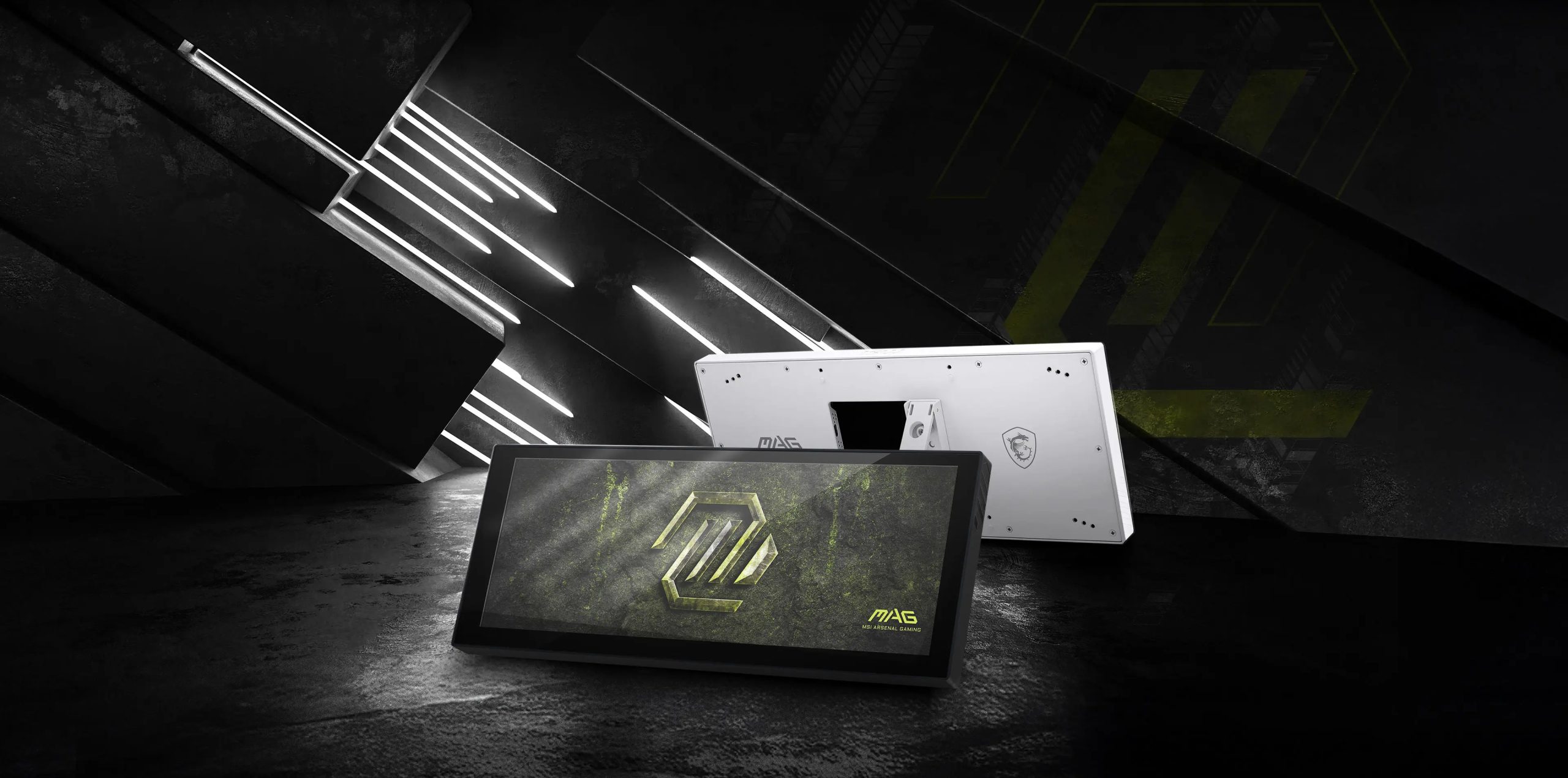
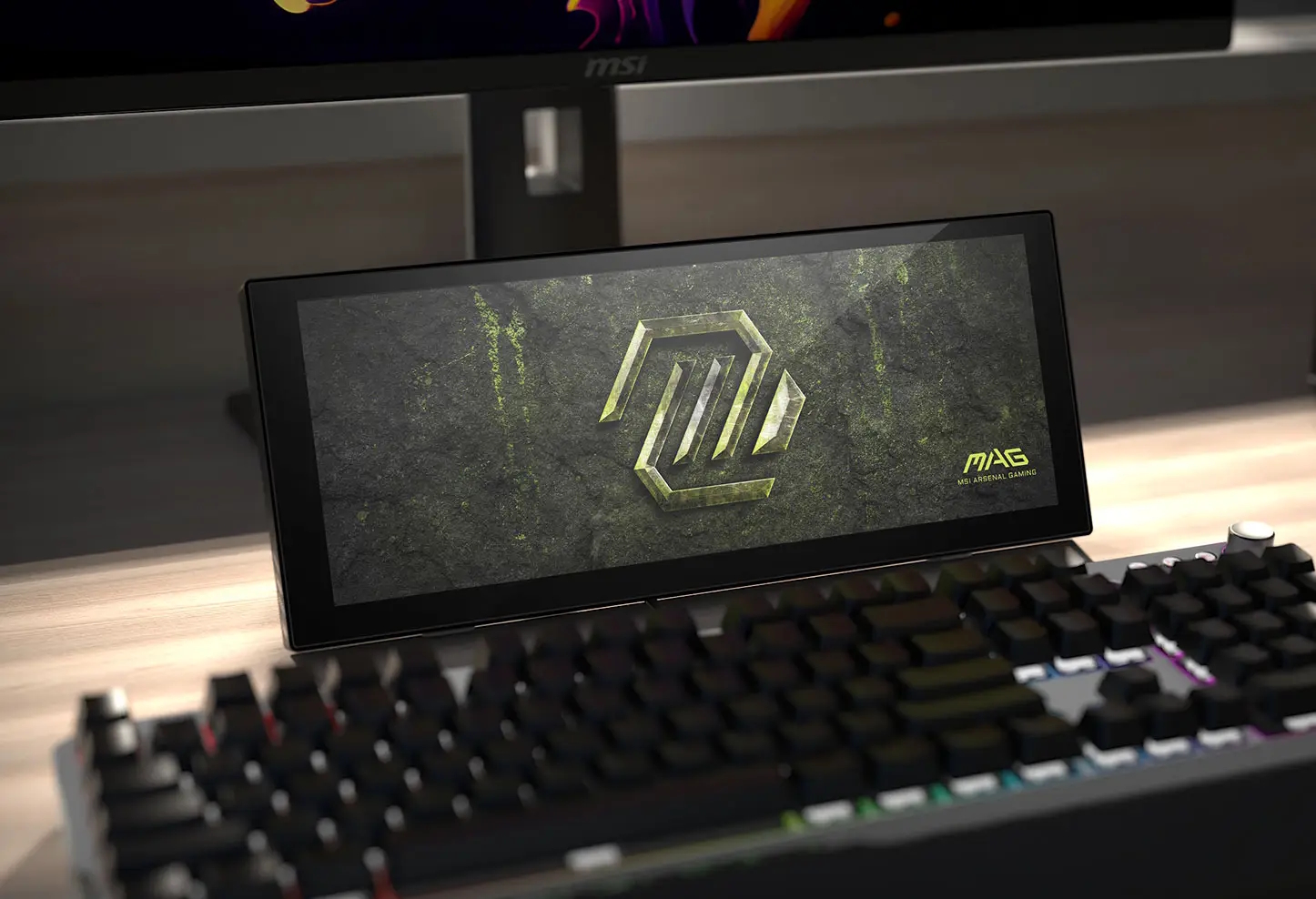
MSI has shared additional details about the MAG View Xpander 12, a 12.3-inch IPS display designed for internal hardware monitoring or as a secondary display in desktop setups.
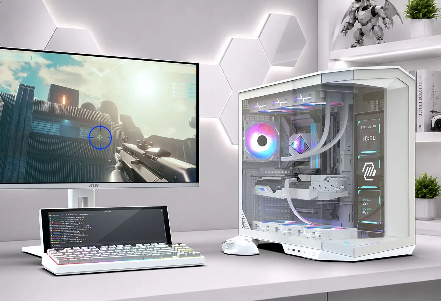
The MAG View Xpander 12 display (via Vortez) features 1920×720 resolution and is available in both black and white finishes. Designed to run in landscape or portrait orientation, the panel integrates with MSI Center software to show system metrics, clock faces, photo slideshows, and custom notifications. Users can also configure the unit as a standard secondary Windows display for chat apps, streaming tools, or reference material.
Installation options include mounting the panel to a 360mm radiator bracket, attaching it to a 120mm fan using an included L-shaped bracket, or placing it on a desk as a standalone monitor. MSI states the screen natively supports select Pano, Velox 300, and Maestro series cases. Power and video signals run over a single USB connection, with both Type-C-to-Type-A and internal USB header cables included in the box.
KitGuru says: MSI is taking on the Xeneon Edge with this new secondary mini-display. Would you like one of these for your setup?
A state-backed company in Shanghai has begun mass-producing immersion deep ultraviolet lithography machines and is due to deliver the first units this year to SMIC, Hua Hong Semiconductor, and memory maker ChangXin Memory Technologies, according to The Information, citing two people familiar with the program. Output targets around five machines in 2026 and roughly 20 in 2027, and all three named recipients sit on the list of Chinese firms that a bill now moving through Congress would cut off from ASML sales and servicing by statute.
The Information didn't name the manufacturer, but its sources described the operation as having pulled DUV development teams from several Chinese companies, one of them the state-backed startup Shanghai Yuliangsheng Technology. SMIC has been testing a Yuliangsheng immersion tool since September 2025. Most components in the new systems are domestic, though some critical parts still come from Japan, and delays at local suppliers have held back output this year.
U.S. House Resolution 8170 designates SMIC, Hua Hong, CXMT, Huawei, and YMTC as restricted entities in law, and three of those five are the named first customers for the domestic scanner. The MATCH Act, introduced in April, was reported out of the House Foreign Affairs Committee on April 22 and has a Senate companion filed as S. 4281. Its immersion DUV provisions cover servicing and technical assistance, not just new exports, which extends its scope to installed tools already operating in Chinese fabs, fabs which have spent the past two years stretching that installed fleet through secondary-channel upgrades.
ASML expects to ship about 130 immersion systems in 2026, matching 2025, CFO Roger Dassen told analysts during the company's July earnings call. Dassen added that ASML intends "to increase capacity by 30% in 2027" for immersion, and is investigating another 30% for 2028. China accounts for around 20% of ASML's net sales this year, down from 33% in 2025, driven mainly by mainstream logic demand.
Immersion DUV prints 28nm-class features in a single exposure and reaches 7nm through multipatterning, at a cost in overlay errors and yield. ASML CEO Christophe Fouquet told the same call that rising DRAM litho intensity partly reflects customers replacing multipatterning with cheaper single-exposure EUV.
Independent analysis from the AI Futures Project in June put commercial-scale Chinese immersion DUV in the mid-2030s, with ASML holding 98.7% of the immersion market. Qualifying the new machines for production lines could take many months, and they trail ASML's tools on performance and build quality. China's domestic EUV effort, which Reuters first reported as a working prototype in December, remains years away.
2026 has been a year of great change at Xbox, with the console maker engaging in a major restructure leading to the parting of ways with 5 different studios and thousands of employees. One notable move made by Xbox was the appointment of Jared Palmer as the new vice-president of engineering. Joining the brand this past May, Palmer has already announced that he is leaving Xbox.
Taking to Twitter, the recently-appointed VP of Engineering at Xbox – Jared Palmer – announced his departure from the company, writing:
“Personal update: I’ve joined @Cognition to lead engineering. I’m grateful to [Asha Sharma] and everyone at Xbox for an amazing year. Excited for this next chapter with [Scott Wu] and team.”
As mentioned, Palmer was a relatively recent addition to the Xbox team, with the announcement happening just a couple months ago in early May. At the time, Palmer was said to be joining “as a member of technical staff to work on product, engineering, developer tools and infrastructure” while also serving as a”taste” maker of sorts.
As with Sharma herself, Palmer came from an AI background, previously serving as the ‘CoreAI vice president of product’ and a ‘senior vice president of Microsoft's GitHub subsidiary.’
Whether his short stint at Xbox was always part of the plan or not, we will have to wait and find out. Either way, this latest change does not lend a great deal of confidence to the new Xbox regime.
KitGuru says: What do you think of this latest move? Is it an indicator of deeper issues? Or did Palmer simply receive an offer he couldn’t refuse? Let us know your thoughts down below.
A new semiconductor firm, TYLsemi (pronounced Tile Semi), publicly revealed itself this month, alongside $43 million in early-stage funding and an ambitious plan to simplify the development of custom processors for AI infrastructure.
Dozens of contract chip designers can develop custom processors of different complexity. However, only a few companies can offer custom silicon design services using standard chiplets to speed up and derisk the development cycle. TYLsemi is aiming to join their ranks. We spoke to their founders to find out how the nascent business might pull it off.
Emerging from stealth
Rather than compete solely as another custom ASIC design house, TYLsemi intends to offer reusable, standards-based connectivity, power delivery, and eventually memory chiplets that customers can combine with their own differentiating compute silicon to build a unique system-in-package. For companies that do not intend to conduct semiconductor development themselves, TYLsemi will also provide an end-to-end service that includes design and implementation of a differentiating chiplet, packaging, qualification, and high-volume production, essentially enabling companies without any silicon development skills to offer their own multi-chiplet processors.
TYLsemi was co-founded by Mohit Gupta and Sunil Bhardwaj, semiconductor veterans who have led global engineering, operations, and business teams at Alphawave, SiFive, Cadence, Rambus, and other chip companies, and who collectively have plenty of experience with both standard and custom silicon. Mohit Gupta, a co-founder and chief executive of TYLsemi, believes that the time to establish a company that specializes in pre-approved chiplets and custom ASIC design is right now.
"Chiplets have been discussed for seven or eight years, but several things have changed in the last three or four years," Gupta told Tom's Hardware Premium. "First, advanced packaging has matured significantly. There are now multiple 2.5D and 3D integration options in volume production. Customers are not limited to one packaging technology or supplier; there are options from foundries and OSATs, including TSMC, Intel, ASE, and Amkor. Second, die-to-die standards have arrived. In the past, most chiplet implementations relied on proprietary interfaces. UCIe is now moving into production deployments, including at hyperscalers, which makes heterogeneous integration much more practical. Third, supply-chain resilience has become critical. Customers increasingly want modular and potentially multi-source strategies rather than a single point of failure. Those factors have created an environment that did not exist four or five years ago."
AI accelerators will be among the primary applications to benefit from multi-chiplet design, as we have already learned from AMD and Nvidia.
"The AI accelerator market is on track to reach $604 billion by 2033, and custom silicon XPUs built for specific hyperscaler workloads are the fastest-growing segment," Gupta said. "At that scale, chiplet-based design is no longer optional, yet there is no pure-play chiplet company serving this market with a full portfolio. TYLsemi closes that gap with standards-based chiplets combined with UCIe-based die-to-die connectivity, XPU-aware design, packaging, and integration — giving customers a fast, proven path to AI-era silicon."
Chiplet economics
The vast majority of AI and HPC accelerators today feature large die sizes, in many cases approaching the size of a reticle. However, as modern process technologies are becoming more complex, foundries tend to increase their quotes for new nodes. A leading-edge wafer used to cost around $15,000 to process around five years ago, but today that price is around $30,000. As a result, large chips at a size close to the reticle limit implemented on a leading-edge node become an option for a select few chip designers who can afford it. For newcomers, multi-chiplet designs enabled by advanced packaging and standardized interconnects such as UCIe start to make a lot more sense.
(Image credit: TYLsemi)
"Once dies get into the 500 – 600 mm² range, the yield curve becomes increasingly difficult. Timing closure on a reticle-sized die is also challenging," Gupta explained. "I have worked on a reticle-sized accelerator, and getting from 99% to the final 1% can require disproportionately more engineering effort."
TYLsemi estimates that its chiplet approach could reduce total cost of ownership by 57% at a volume of 100,000 devices, from $350 million for a monolithic 700 mm² 3nm-class chip to $150 million for a design combining a 500 mm² 3nm-class compute die with four 100 mm² I/O chiplets built on an N-1 process. TYLsemi believes that the unit price of a monolithic chip would be $3,000, whereas the cost of an SiP would be around $600. The company attributes the saving to higher yields, reusable I/O silicon, lower IP licensing and engineering costs, and substantially lower per-unit silicon costs. However, the company stresses that the figures are illustrative estimates rather than actual manufacturing costs. Additionally, multi-chiplet designs can enable faster product refreshes compared to large monolithic dies as they are faster to develop and yield.
"Compute may move to 2nm or A14, while high-speed I/O can remain on 3nm, since I/O does not scale in the same way as logic," Gupta said. "Our power-delivery chiplets can use an even less advanced process. Customers therefore do not have to use the most expensive silicon real estate for every function. […] There is no single answer for every design. You have to determine the right disaggregation points based on the architecture, thermal requirements, package, and how multiple accelerators communicate. […] The exact partitioning will vary by application, but you still get a better total cost of ownership."
TYLsemi primarily targets AI infrastructure, so it generally envisions multi-chiplet designs to be used for AI accelerators, data-center CPUs, high-performance computing, networking and telecom silicon, and heterogeneous SoCs. However, TYLsemi has also ignored the fact that multi-chiplet designs are already widely used for consumer CPUs and GPUs.
Foundation chiplets
At the core of TYLsemi's proposition are its foundation chiplets, which are reusable building blocks intended to handle common non-compute functions in custom AI and infrastructure processors and are implemented using various process technologies from TSMC. The foundation chiplets include the following:
(Image credit: TYLsemi)
TYL.IO — a family of connectivity chiplets that includes TYL. IO PCIe, a 32-lane PCIe 7.0/CXL chiplet connected to the compute die via UCIe; TYL.IO Scale, a 224G+ SerDes for ESUN/UALink scale-up connectivity; and TYL.IO EIC for co-packaged optics.
TYL.Power — a 16nm in-package IVR chiplet with embedded passives, designed to provide power closer to compute dies and use closed-loop control and die telemetry to improve power delivery.
TYL.Mem — a planned family of memory-connectivity chiplets. TYLsemi has not yet disclosed the architecture or specifications, though it is safe to assume they are talking about memory controllers and PHYs.
Not all of these chiplets will be available immediately, as the company has certain priorities amid limited resources.
"The first TYL.IO product disaggregates the PCIe functionality that would normally sit on a large server processor, it is a 32-lane PCIe Gen7/CXL chiplet connected to the host compute die using UCIe," Gupta explained. "The idea is that the CPU cores can move to 2nm, A14, or another leading-edge process, while the I/O chiplet remains on 3nm. The next product in the family will address scale-up connectivity between XPUs within a rack using high-speed SerDes. That device will be considerably larger, with around 72 lanes and approximately 14 TB/s of bandwidth. We also have an EIC roadmap for co-packaged optical connectivity. We expect samples of our first I/O product in the second half of 2027."
These chiplets can be used as standalone components or integrated with a customer's compute dies designed by the customer to TYLsemi through TYL.Forge, TYLsemi's end-to-end custom silicon platform.
TYL.Forge
TYL.Forge is arguably one of the key enablers of TYLsemi's business, as the program is aimed at companies that have their own compute architecture or even a compute die, but cannot build their own SiP or manage the entire semiconductor supply chain.
"There are larger custom silicon companies in the market, but many of them focus on a relatively small number of customers that can generate billions of dollars in annual business," Gupta explained. "We see an opportunity among emerging AI companies and system companies that need advanced custom silicon but also need a partner capable of taking responsibility for the entire implementation and supply chain."
(Image credit: TYLsemi)
Such clients can provide their proprietary compute RTL, while TYLsemi handles physical implementation and integrates the resulting compute die with its pre-validated connectivity, power, and eventually memory chiplets. The company then manages tape-out, packaging, assembly, testing, qualification, and high-volume production.
"For example, a customer building a large accelerator can bring us its matrix-multiplication engine," Gupta said. "We can implement the custom compute die and integrate it with our chiplets, so the customer does not have to reinvent the I/O and other common functions. This reduces risk and time to market."
In fact, TYL.Forge appears flexible about where the customer enters the development process. TYLsemi describes the platform as covering everything from architecture and front-end design through implementation, tape-out, assembly, qualification, and production. So instead of RTL, customers can come to TYLsemi with an architecture/concept, and then the company will help develop and implement the silicon. Nonetheless, TYLsemi does not intend to invent the customer's core compute architecture itself. In addition, customers can bring in an existing compute die, which TYLsemi can combine with its chiplets, package, test, and bring to production.
"We are also talking with companies developing Arm- and RISC-V-based server processors," Gupta said. "They can develop the architecture, while we implement the rest of the silicon and bring the product to production. That gives customers an economic and engineering advantage because they do not need to build teams for every part of the chip."
The key advantage of TYL.Forge is the reuse of pre-validated components. Instead of developing common functions such as PCIe connectivity and power delivery for every new processor, customers can use TYLsemi's pre-validated foundation chiplets and focus engineering resources on differentiated compute architectures, software, and system design. In theory, TYLsemi could integrate third-party chiplets (not from a customer, but from a third-party chiplet provider). Still, the company's focus remains on offering its own pre-validated chiplets and custom silicon with SiPs it builds.
"Potentially, [we could integrate third-party UCIe chiplets into a TYLsemi-based system], UCIe has done a very good job defining the electrical interface, but the ecosystem is still maturing at the protocol level," Gupta explained. "In some cases, if we provide a chiplet to a customer, we may also need to provide or enable the UCIe IP on the other side of the connection. We are committed to UCIe and industry standards because standardization ultimately wins. […] We can consider customization for a large strategic customer or hyperscaler, but we do not want those projects to derail our standard product roadmap. […] Even when customers buy our standalone chiplets, I expect many of them will ask us to handle packaging and testing because heterogeneous integration and supply-chain management are difficult "
TYLsemi estimates that its approach can cut development time and cost by up to 50% compared with traditional custom silicon programs. In the best-case scenario, TYLsemi envisions that the development cycle can shrink considerably compared to today's cycles that can be two, three, or more years long. According to TYLsemi, once a customer provides sufficiently mature RTL or a netlist, the company can take a custom compute die to tape-out in around six to nine months or so, which includes fabrication, assembly, testing, and qualification.
"If a customer provides mature final RTL or a netlist and uses our standardized I/O chiplet, we believe we can take the custom compute die to tape-out in approximately six months in some cases," Gupta explained. "More generally, our target is six to nine months from a mature design to tape-out. The architecture and front-end phase is more customer-dependent. For a first-generation product, that can take around six months; for a more mature second- or third-generation design, it could be closer to three months, and some of that work can overlap with implementation. After tape-out, fabrication can take roughly four to five months depending on the process, followed by perhaps another two months for assembly, testing, and qualification. If the architecture is already mature, it may therefore be possible to reach production samples in about a year."
Still, the company stresses that architecture development and implementation typically include feedback loops, which greatly slow the development process. This is why the company provides the relatively conservative '50%' figure.
TYL.IO and TYL.Power samples will be available to qualified customers in 2027, in partnership with TSMC, and the company is looking forward to designing processors for its clients in time for them to reach the market in 2029 – 2030.
Speaking of TSMC, TYLsemi will initially only offer designs and services adhered to the TSMC ecosystem, though eventually it may offer other options for packaging technologies, such as Intel's EMIB and Foveros, or Amkor's packaging methods.
"We are initially focused on the TSMC ecosystem, but we also intend to explore other advanced-packaging supply chains," Gupta said. "We do not want to limit ourselves to one packaging option. Over time, that could include other OSATs and packaging technologies. […] That could include Intel, ASE, Amkor, or others. Amkor, for example, is building significant packaging capacity in Arizona."
Intel will design, package, and fabricate Fortinet's sixth-generation Security Processor (SP6) on its Intel 4 node, the companies announced on July 21, giving the process its first named external foundry customer, roughly three years after it entered production. Intel told Tom's Hardware the agreement reflects "the strategy Intel outlined for Intel 4 several years ago," including support for custom networking ASIC workloads. Intel's own record from those years reads differently, however, with the company's 2021 roadmap having scoped Intel 4 to two internal products. And through 2022, it told engineers and investors that Intel 3, not Intel 4, would be its first process offered to foundry customers.
Intel 4's record
Intel's Accelerated announcement back in July 2021 said that Intel 4 would reach production readiness in the second half of 2022 for products shipping in 2023, naming "Meteor Lake for client and Granite Rapids for the data center." The release and its accompanying fact sheet, however, contained no reference to foundry customers, networking, or custom ASICs on the node.
At VLSI 2022, Intel disclosed that it wasn't building a high-density library for Intel 4 and that Intel 3 would be the first new node offered through what was then Intel Foundry Services. A 2024 post on Intel's own foundry blog describes Intel 3 as "Intel Foundry's first leading-edge process node," and Intel's fiscal year 2024 annual report listed the processes available to external customers as 18A, Intel 3, Intel 7, Intel 16, and a 12nm node co-developed with UMC. Intel 4 appears nowhere on that list.
Ericsson's RAN Compute processors, announced in November 2023, were built on Intel 4, so Fortinet's part won't be the first third-party silicon to come off the node. That work grew out of a bespoke Intel-Ericsson collaboration, though, and Ericsson's formal foundry agreement with Intel, announced in July 2023, covered 18A. Fortinet is the first named customer buying Intel 4 as a foundry service, and the first cybersecurity vendor on any Intel node. The Ericsson engagement is also the closest thing in the public record to networking silicon on Intel 4, two years after the strategy Intel now says it outlined for the node.
Fab 34 economics
Intel 4 entered high-volume manufacturing at Fab 34 in Leixlip, Ireland, in September 2023, producing the compute tile for Meteor Lake-based Core Ultra chips, and shares the fab with Intel 3. Intel sold a 49% stake in the facility to Apollo-managed funds for $11.2 billion in June 2024, then bought it back in April 2026 for $14.2 billion, funded with $7.7 billion in cash and $6.5 billion in new debt. That buyback returned 100% of Fab 34's wafer economics to Intel at a premium of roughly 27%, and it only pays off if the fab's EUV capacity stays loaded.
Meteor Lake is aging out of Intel's lineup as 18A-based Panther Lake ramps through 2026, which leaves open the question of what fills Intel 4 capacity next. A multi-generation firewall ASIC program is a reasonable answer with mature yields, a customer that values supply stability over bleeding-edge density, and a part Intel described as tailored for cost-sensitive applications. Intel said in April that yields were improving across Intel 4, Intel 3, and 18A.
Fortinet's supply chain
Fortinet's 2025 annual report names Renesas and Toshiba America as the contract manufacturers for its ASICs, utilizing foundries in Taiwan and Japan operated either by TSMC or by the contract manufacturers themselves. The current SP5, a monolithic 7nm Arm-based SoC announced in February 2023, sits in that supply chain, so SP6 on Intel 4 moves Fortinet's next flagship security processor out of a TSMC-linked flow and into Intel's. The disaggregated design language in the announcement points to a chiplet-based part, a first for Fortinet's SP line.
Fortinet re-engineered three FortiGate models in 2022, the 70F, 600F, and 3700F, to accept alternative components during the chip shortage, and CMO John Maddison told SDxCentral at the time that the company wouldn't wait for parts to arrive in 2023. The "resilient and diversified" supply chain used in the SP6 press tracks back to that experience. Ken Xie called Fortinet "the #1 firewall leader with a 55% unit market share" in the company's 2025 results in February, with approximately six million FortiGates deployed, so there’s real, substantial volume here even if the parts are relatively inexpensive.
Intel Foundry reported $307 million in external revenue for 2025, up from $159 million the year before, against total foundry revenue of $17.8 billion and an operating loss of $10.3 billion. External revenue in Q1 2026 was $174 million. Fortinet's hardware business runs at roughly 30% of its revenue, and, per analysis from ServeTheHome, SP6 is ultimately a component of a portion of an annual hardware stream around $2 billion, so the deal won't move Intel's foundry line materially, even at full production.
CEO Lip-Bu Tan told CNBC in May that he expected commitments from multiple foundry customers in the second half of 2026, and Intel told investors in January that two prospective customers were evaluating 14A test chips. The SP6 announcement comes inside Tan's stated window, and it finally gives Intel something its foundry marketing has lacked in a named customer with shipping volume on a node with mature yields. Meanwhile, an 18A or 14A commitment from a major external customer is still missing, and Fortinet's cost-sensitive parts on a 2023 node don't substitute for one.
NVIDIA is addressing the biggest concerns regarding DLSS 5 while presenting the tools it offers to developers to retain "artistic integrity" at SIGGRAPH. NVIDIA Says DLSS 5 Is Not "AI Replacing Graphics" but rather "AI Expanding Graphics", As It Promises More Control To Preserve Artists' Vision While Delivering Enhanced Visuals At GTC 2026, NVIDIA unveiled DLSS 5, its next major update to the DLSS technology suite. The first DLSS off vs DLSS on comparisons showed a day-and-night difference in visuals, massively uplifting the quality of existing assets through Neural Rendering, but as soon as the technology was unveiled, there was […]
Intel and Fortinet have announced a strategic collaboration to develop the Fortinet Security Processor 6 (SP6), the next generation of the custom silicon behind Fortinet's FortiGate firewalls. Intel will contribute chip design, advanced packaging, and manufacturing to the SP6 program, making Fortinet the first cybersecurity vendor named as an Intel silicon customer.
Intel told Tom's Hardware that SP6 will be built on Intel 4, the EUV process the company has so far used only for its own products, making Fortinet both the first cybersecurity vendor named as an Intel silicon customer and the first named external customer for the node. However, the announcement specifies no production timeline, and it comes in the same Q3-Q4 2026 window in which CEO Lip-Bu Tan said the company expects commitments from multiple foundry customers.
SP6 will draw on what the companies described as Intel's expertise in disaggregated semiconductor design and advanced packaging tailored for both AI-enabled and cost-sensitive applications.
That points to a chiplet-based part, which would be a departure from the current SP5, a monolithic 7nm Arm-based SoC that Fortinet launched in 2023 for its entry-level and mid-range FortiGate appliances. The deal will help Fortinet "accelerate and strengthen our ASIC strategy," said Ken Xie, founder, chairman, and CEO of Fortinet, in the announcement.
Intel 4 was the company's first process node to use EUV lithography and entered high-volume manufacturing at Fab 34 in Ireland in September 2023, where it produces the compute tile for Meteor Lake-based Core Ultra chips. The node didn't appear among the processes Intel listed for external foundry customers in its fiscal year 2024 annual report, which named 18A, Intel 3, Intel 7, Intel 16, and a 12nm process co-developed with UMC. Intel said the SP6 work reflects plans it laid out for Intel 4 several years ago, including support for custom networking ASIC workloads.
Microsoft agreed in early 2024 to build an unnamed custom chip on Intel's 1.8nm-class 18A node, a deal that reportedly covers a next-generation Maia AI processor. That announcement followed a similar pattern, with no product details, node variant, or timeline at signing and specifics emerging over the following 18 months.
Intel CFO David Zinsner said in March that the company was fielding inbound interest in 18A-P from prospective foundry customers as yields improved, and Tan told CNBC in May that foundry commitments were expected in the second half of 2026.
Fortinet does bring real volume, though, if not marquee volume. IDC ranked Fortinet first in firewall appliances shipped as of early 2023, with a 48% unit share. The company ships its own ASICs across its entry-level and high-end FortiGate ranges, and SP6 extends a silicon program now in its sixth generation.
Neither company committed to work beyond SP6, though the release described the agreement as a starting point, with further collaboration on chip technology and manufacturing under discussion.

 Login
Login