Reading view

There are new articles available, click to refresh the page.

MSI XpertStation WS300 Thermals: Why a 1,300W GB300 Doesn’t Throttle on a Desk
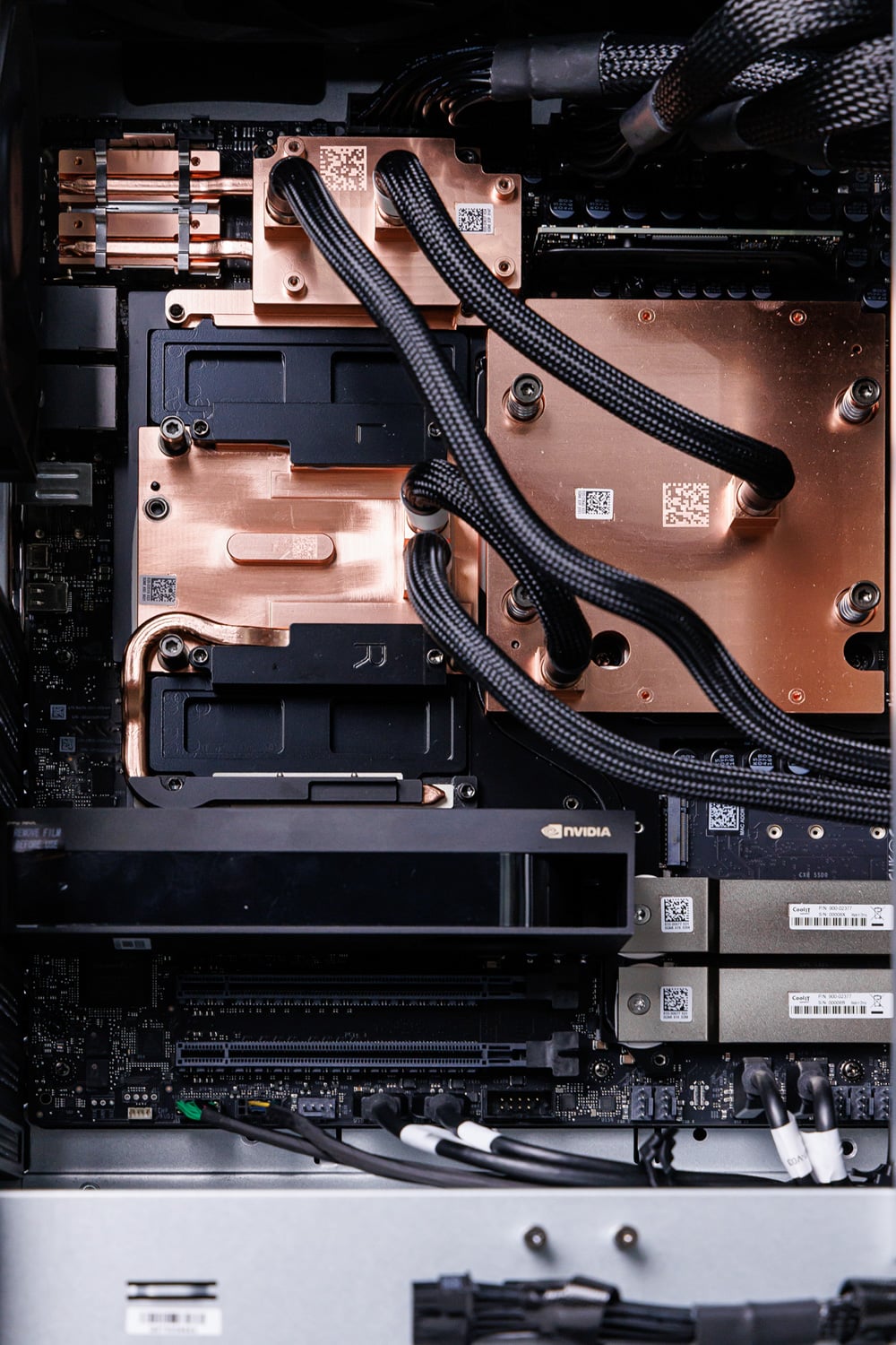
Power delivery in the MSI XpertStation WS300 with its 1,600W 80 PLUS Platinum supply Power delivery in the MSI XpertStation WS300 with its 1,600W 80 PLUS Platinum supply

The most common question we got about the MSI XpertStation WS300 after our review coalesces around one key theme. The GB300 Grace Blackwell Ultra Superchip is a 1,300W part that normally lives in a liquid-cooled rack, so what happens to thermals when you put it in a tower? The concern is fair: a GB300 system that hits its thermal limit will shed performance, and a system that throttles under sustained inference isn’t delivering what it was bought for. In our review, we said the WS300 stayed cool and stable through testing. The why is in MSI’s own cooling design data, paired here with the thermal, power, and clock traces we logged during a run on the system.
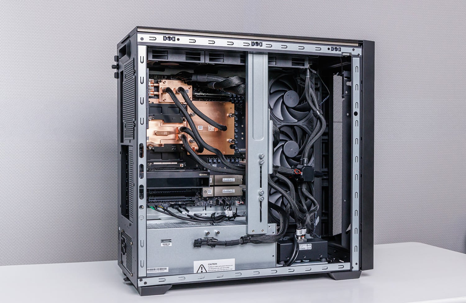
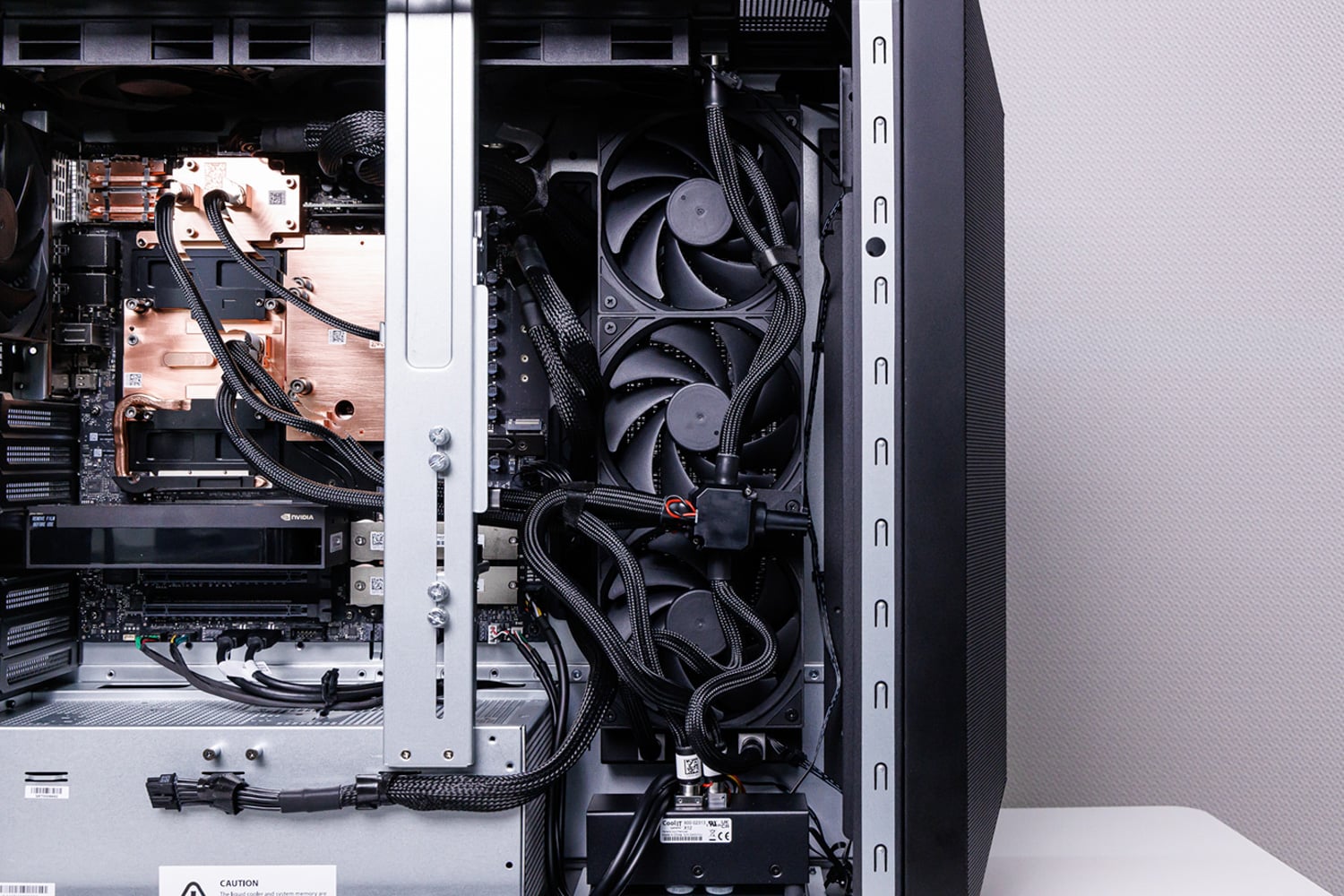
Inside the MSI XpertStation WS300: copper cold plates over the GB300 Superchip, SOCAMM memory, and ConnectX-8 with braided coolant tubing

What the Loop Has to Do

The thermal budget on a DGX Station is set by NVIDIA; the GB300 module carries a 1,300W SuperChip power limit, and the whole system runs from a single 1,600W power supply that also has to feed storage, pumps, fans, and any optional RTX PRO card. Nearly all of that 1,300W ends up as heat in four places: the Blackwell Ultra GPU and its 252GB of HBM3e, the 72-core Grace CPU, 496GB of memory across four SOCAMM LPDDR5X modules, and the ConnectX-8 SuperNIC with its two 400GbE optical ports. MSI puts cold plates on all four, and the loop runs through two 360mm radiators with six 120mm fans. A separate 120mm chassis fan moves air through the rest of the case for the SSDs and other air-cooled parts. MSI rates the assembly for 1,400W across the CPU and GPU, roughly 100W above what NVIDIA lets the Superchip draw.

That 100W of margin is a design decision that matters quite a bit. A loop rated only for the nominal load has no room for a warm office, a dusty radiator, or a fan running below full speed. A loop with headroom above the power limit means the silicon reaches its power cap before it reaches its thermal cap.

MSI’s Cold Plate Data

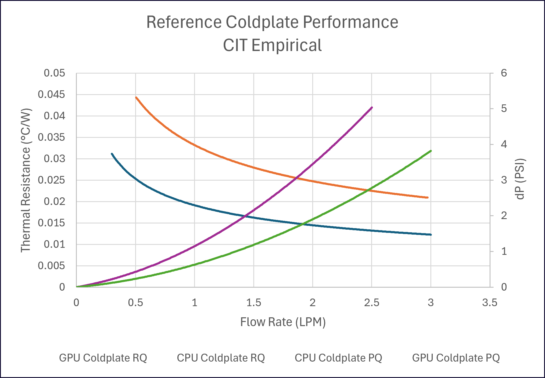
MSI shared the characterization data behind the loop with us. The company calls the methodology CIT, for Component Integrity Test, and labels the curves empirical: they were measured on the bench across repeated pressure and thermal cycles. The first chart is the one a thermal engineer cares most about. It plots thermal resistance in degrees C per watt for the GPU and CPU cold plates against coolant flow rate, along with the pressure drop each plate imposes on the pump.
MSI XpertStation WS300 cold plate performance chart: GPU and CPU cold plate thermal resistance and pressure drop versus coolant flow rate

The GPU plate starts near 0.031 C/W at a trickle of 0.3 liters per minute and drops steeply as flow increases, reaching about 0.017 C/W at 1.5 LPM and 0.012 C/W at 3 LPM. The CPU plate, which covers a much lower-power part, sits higher, around 0.028 C/W at 1.5 LPM. Thermal resistance is the multiplier that turns watts into degrees: at 1.5 LPM, every 100W through the GPU plate costs about 1.7C of rise between the coolant and the plate. Push 1,000W through it, and the plate runs about 17C above the water. The tradeoff is pressure drop, which climbs with the square of flow. At 1.5 LPM, the GPU plate costs the pump about 1.1 PSI and the CPU plate about 1.9 PSI. The curves flatten past 2 LPM, which is why the loop is designed to run in the 1.5 to 2 LPM range; higher flow buys a diminishing thermal return for a steep pump cost.

Radiators, Fans, and the Noise Trade-off

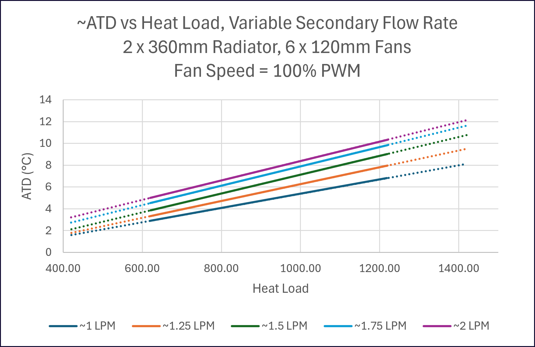
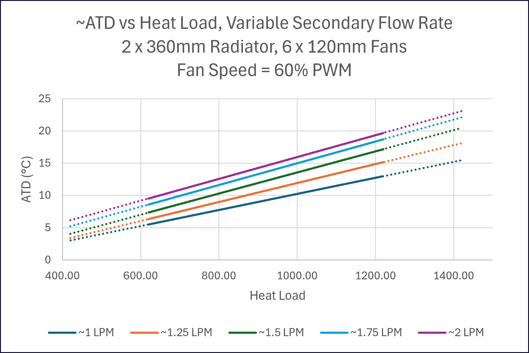
The second set of charts covers the other end of the loop. ATD is the term for Ambient Temperature Difference, the rise of the coolant above room air after it leaves the radiators. It’s the number that sets the floor for every component temperature in the system, since nothing on the loop can run cooler than the water feeding it. MSI plots ATD against heat load for the pair of 360mm radiators at flow rates from 1 to 2 LPM, once with the six fans at 100 percent PWM (pulse-width modulation) and once at 60 percent.
MSI XpertStation WS300 radiator approach temperature chart at 100 percent fan PWM: coolant rise over ambient versus heat load for 1 to 2 LPM flow

At full fan speed, the radiators hold the coolant within 5 to 9C of ambient at a 1,000W heat load across the flow range, and within 8 to 12C at 1,400W, past the Superchip’s power limit. The lines are nearly linear, and slower coolant spends longer in the radiator and comes out closer to room temperature, which is why the 1 LPM line sits lowest; the tradeoff is the higher cold plate resistance at low flow from the first chart, so the loop’s operating point is a balance between the two. The 60 percent PWM chart is the more realistic one for a system beside a desk, because nobody runs (or wants to run) six 120mm fans flat out in an office.
MSI XpertStation WS300 radiator approach temperature chart at 60 percent fan PWM: coolant rise over ambient versus heat load for 1 to 2 LPM flow

At 60 percent, ATD roughly doubles: 10 to 16C at 1,000W and 15 to 23C at 1,400W, a relatively modest penalty. Even at full Superchip power and reduced fan speed, the coolant enters the cold plates no more than about 23C above the room. Add the 17C GPU plate rise from the first chart, and the Blackwell Ultra package is running around 40C above ambient at 1,000W, well inside its operating range in any normal office. The final MSI chart is the radiator’s air-side impedance curve, which shows the pressure the fans have to overcome to push air through the fin stack, reaching about 1 mm of water at 135 CFM and 2 mm at 185 CFM. It’s a low-restriction core, which is what lets the fans run slow.
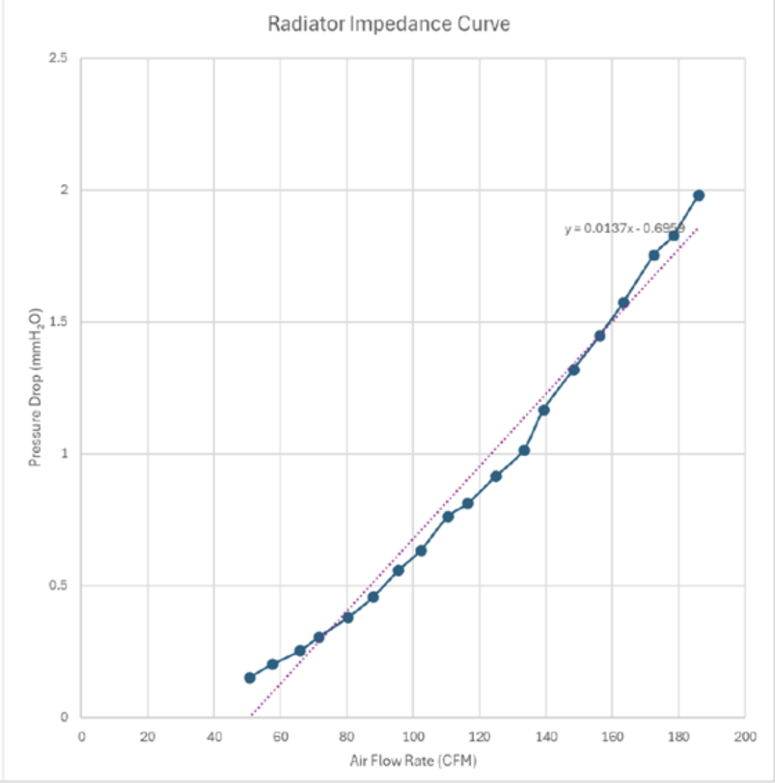
MSI XpertStation WS300 radiator air impedance curve: pressure drop in mm of water versus air flow in CFM
Liquid cooling radiator, fans, and braided tubing inside the MSI XpertStation WS300

Our Run: ~3 Hours on the GB300

Design curves say what a loop should do, to see what it actually does, we logged the WS300 through a 2.8 hour session made up of five phases: a 75 minute burn-in at sustained GPU load, then DeepSeek v4 Flash served through vLLM under three profiles, an equal 512 input and 512 output token workload, a prefill-heavy 8,192 in and 1,024 out workload, and a decode-heavy 1,024 in and 8,192 out workload stepped through increasing concurrency, followed by an idle observation window. We sampled the GPU, HBM, CPU, and power telemetry continuously. Coolant, chassis air, and board temperatures come from the BMC, which we polled every couple of minutes. The shaded regions in each chart mark the phases.
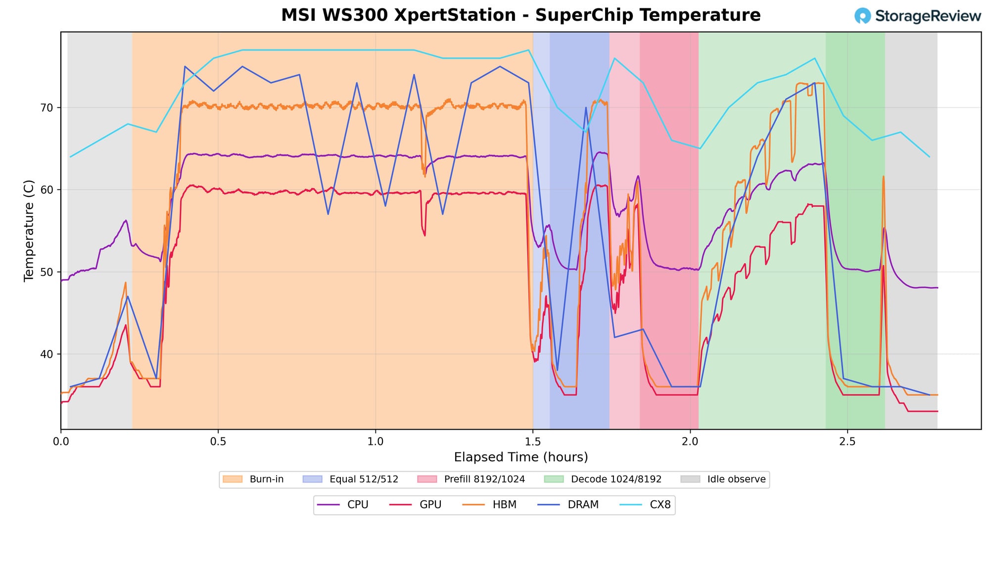
MSI XpertStation WS300 Superchip temperature chart over a 2.8 hour run showing CPU, GPU, HBM, DRAM, and ConnectX-8 temperatures across burn-in, three DeepSeek v4 Flash inference phases, and idle

Through the entire burn-in, the Blackwell Ultra die was held at 60C, with HBM3e about 10C warmer at 70C and Grace at 64C. Those are the steady-state numbers at roughly 1,000W of GPU power, and they didn’t drift upward over the 75 minutes, which is the signature of a loop that has reached equilibrium with headroom. The inference phases are cooler on average because the load is burstier: the GPU peaked at 60C again during the equal workload and 58C during the long decode ramp, with HBM topping out at 73C. The sawtooth on the DRAM line is an artifact of the BMC’s sampling interval; the LPDDR5X itself peaked around 75C. The warmest sensor in the box for most of the run was the ConnectX-8 at 76 to 77C. Idle temperatures settled at 33 to 36C for the GPU and HBM and around 48C for Grace.
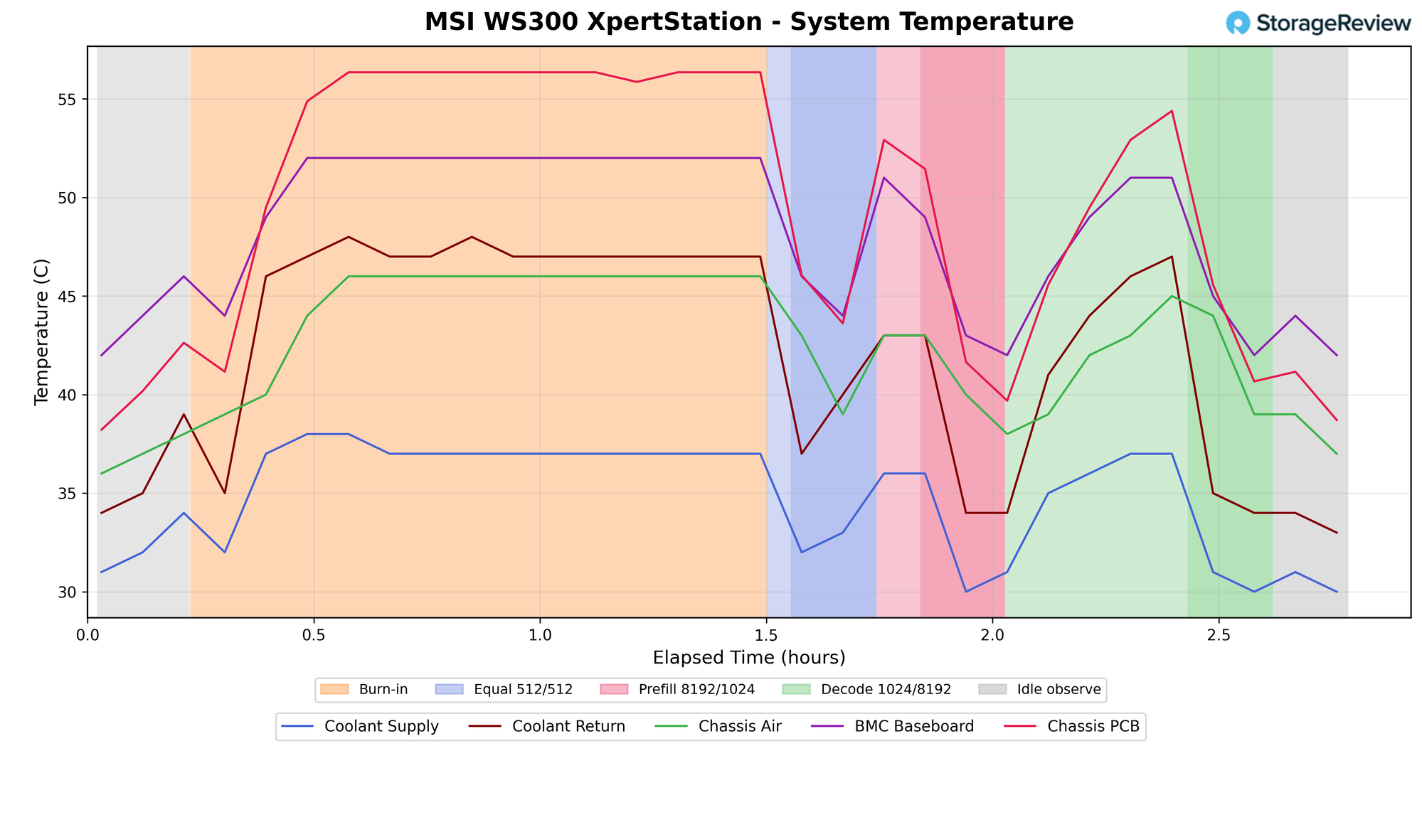
MSI XpertStation WS300 system temperature chart showing coolant supply and return, chassis air, BMC baseboard, and chassis PCB temperatures across the 2.8 hour run

During burn-in, the coolant left the radiators at 37C and returned from the cold plates at 47C, a 10C rise across the loop. Chassis air inside the case reached 46C, the BMC baseboard 52C, and the hottest board sensor 56C. Every one of those lines plateaus within the first 15 minutes of load and stays flat, then falls back within minutes when the load stops. At idle, the coolant supply sat at 30 to 31C.
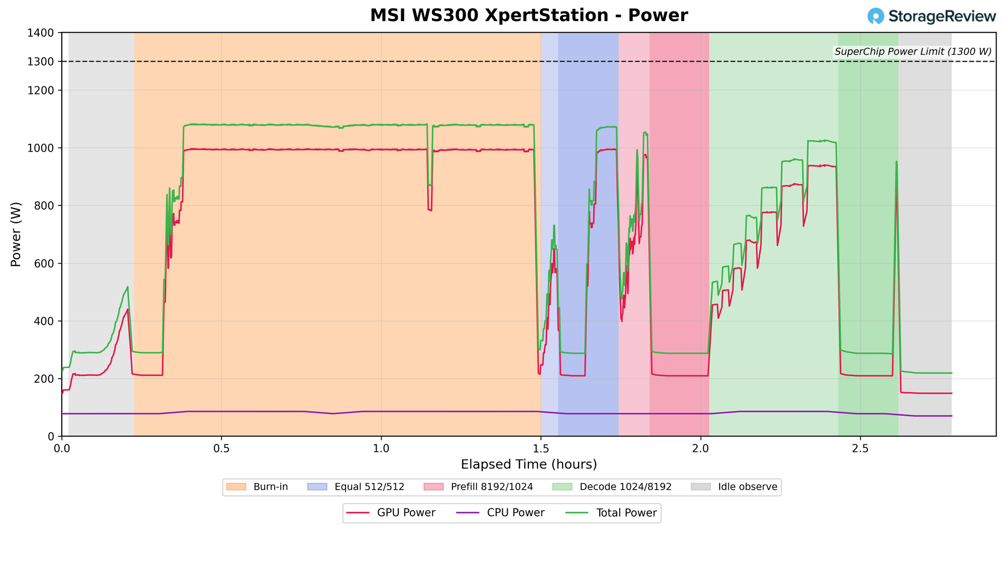
MSI XpertStation WS300 power chart showing GPU, CPU, and total Superchip power against the 1,300W limit across burn-in, inference, and idle phases

Burn-in held the GPU at about 995W, with Grace adding another 85 to 90W for a Superchip total near 1,080W, which is the load the coolant delta above corresponds to. The equal workload briefly touched the same 1,000W GPU level at high concurrency; the prefill-heavy phase ran in short bursts to about 1,050W total; and the decode-heavy ramp is the clearest picture of how an inference server loads a GPU, stepping from roughly 500W to just over 1,000W as concurrency doubled at each stage. At no point in the run did total Superchip power come within 200W of the 1,300W limit marked on the chart. Idle is worth noting for anyone planning power: the GPU alone draws 150 to 210W with nothing running, and the Superchip total idles at 220 to 290W.
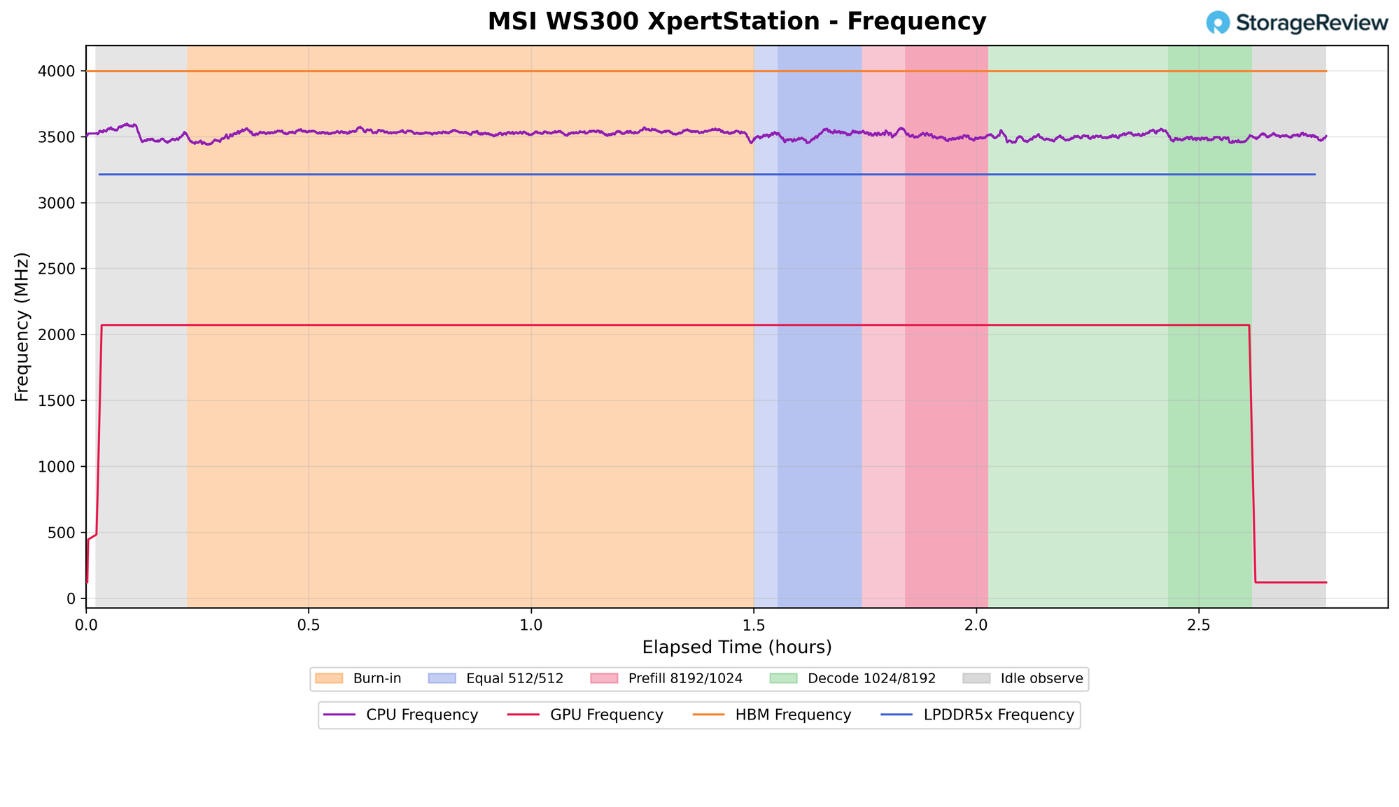
MSI XpertStation WS300 frequency chart showing GPU clock flat at about 2.07GHz, CPU near 3.5GHz, HBM at 4,000MHz, and LPDDR5X at 3,200MHz across the full run

The Blackwell Ultra ran at about 2.07GHz from the moment the burn-in started until the run ended, a flat line through every phase with no dips at all. Grace held near 3.5GHz with normal jitter, HBM stayed at 4,000MHz, and the LPDDR5X stayed at 3,200MHz. A thermally limited GPU shows up here as very choppy, as the boost algorithm backs off and recovers; a power-limited one shows up as a clock that tracks load; neither pattern appears in our testing. Under these workloads, the system was neither hot enough nor power-constrained enough to leave its top clock.

Tying the Two Together

MSI’s curves and our measurements were produced independently, and they come together at the same conclusion. Start from the 10C coolant rise at 1,080W. Heat carried by a liquid is flow times temperature rise, so that delta implies a coolant flow rate of about 1.5 liters per minute for water-based coolant, squarely in the range MSI characterized. Read MSI’s radiator chart at that flow and load: at 100 percent fan speed, the coolant should sit about 8C above the room; at 60 percent, about 14C. We didn’t have a calibrated ambient probe in MSI’s lab, so we can’t close that loop to the degree, but a 37C supply temperature is consistent with a warm lab room and fans running well below full speed.

At 1.5 LPM, the GPU plate’s measured resistance is about 0.017 C/W, which at 995W predicts a 17C rise from coolant to plate. We measured the Blackwell Ultra die at 60C against a 37C supply, a 23C gap. The 6C difference between the two is the thermal interface and the package itself, the part of the path the cold plate can’t control, and it is a small number for a dual-reticle GPU of this size. The plate is doing what MSI’s bench data says it does, and the margin between the die and the coolant is dictated by physics.

Work the budget the other way, and the headroom we discussed earlier becomes more visible. NVIDIA’s data center GPUs don’t begin reducing clocks until the die is well into the 80s, so the WS300 at full sustained load left roughly 20C between the Blackwell Ultra die and the point where thermal management would step in, and that was with the loop absorbing 1,080W. Even at the worst-case 1,300W Superchip limit, another 220W through a 0.017 C/W plate adds under 4C at the GPU, and MSI’s radiator chart shows the coolant rising only about 2C more for that extra load.

What This Means for a Buyer

The WS300 doesn’t throttle under sustained inference or synthetic load because its cooling loop was sized above the Superchip’s power limit, and the measured temperatures leave roughly 20C of margin at the GPU, with HBM and CPU running cooler still relative to their limits. The component that runs warmest is the ConnectX-8, which is why it’s on the loop in the first place. Coolant temperatures stabilize within 15 minutes and recover within minutes, so back-to-back jobs don’t stack heat. Fan speed is the one lever between noise and coolant temperature, and MSI’s 60 percent data shows the system can give up a lot of airflow before the fans have to scale up. The one thing that doesn’t shrink is the electrical side: a 20A circuit is still required in North America, and idle draw in the 220 to 290W range is the cost of keeping 252GB of HBM3e and a 72-core Arm CPU ready to work. Then again, with this kind of investment, the system should rarely be kept idle.

This report is sponsored by MSI. All views and opinions expressed in this report are based on our unbiased view of the product(s) under consideration.

MSI XpertStation WS300 Product Page

The post MSI XpertStation WS300 Thermals: Why a 1,300W GB300 Doesn’t Throttle on a Desk appeared first on StorageReview.com.
Fujitsu MONAKA Server Brings 2nm 144-Core CPUs to Air-Cooled AI Inference, On Sale in November

Fujitsu MONAKA Server Fujitsu MONAKA Server

Fujitsu is bringing its 2nm FUJITSU-MONAKA processor to AI infrastructure with a new server family designed to run AI inference in air-cooled data centers without requiring specialized liquid cooling. The MONAKA Server is designed, developed, and manufactured in Japan, with component and manufacturing traceability for sovereign AI deployments.

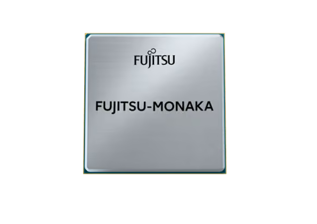
FUJITSU-MONAKA CPU package render with the Fujitsu logo, the 2nm 3D-stacked processor at the heart of the Fujitsu MONAKA Server

The first MONAKA Servers will come in 1U and 2U configurations for AI inference and AI agents, with a separate 2U multi-node system planned for academic and HPC environments. Fujitsu is also making the MONAKA processor available separately for cloud and data center operators and other server vendors.

MONAKA runs at up to 3.8GHz and supports memory transfer speeds up to 8800MT/s, with dedicated matrix instructions and SVE2 vector processing accelerating AI inference directly on the CPU. Fujitsu rates MONAKA at twice the AI inference throughput of other CPUs, although it hasn’t identified the processors used for that comparison or provided benchmark results.

MONAKA Brings AI Inference to Air-Cooled Servers

The 1U MONAKA Server supports air cooling at ambient temperatures up to 40 degrees Celsius, while its liquid-cooled configuration supports water temperatures up to 45 degrees Celsius.

Fujitsu rates its server cooling technology for up to an 80% reduction in cooling power consumption, although specific system configurations and test conditions weren’t provided. The air-cooled configuration is particularly interesting for data centers that want to add AI inference capacity without changing their existing cooling infrastructure.

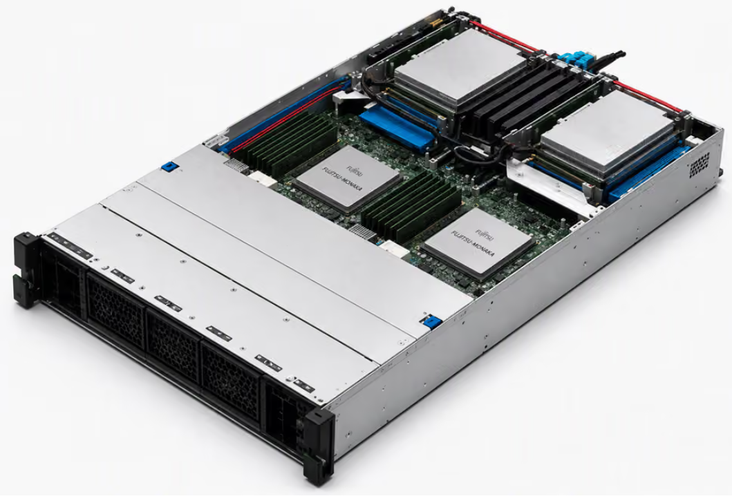
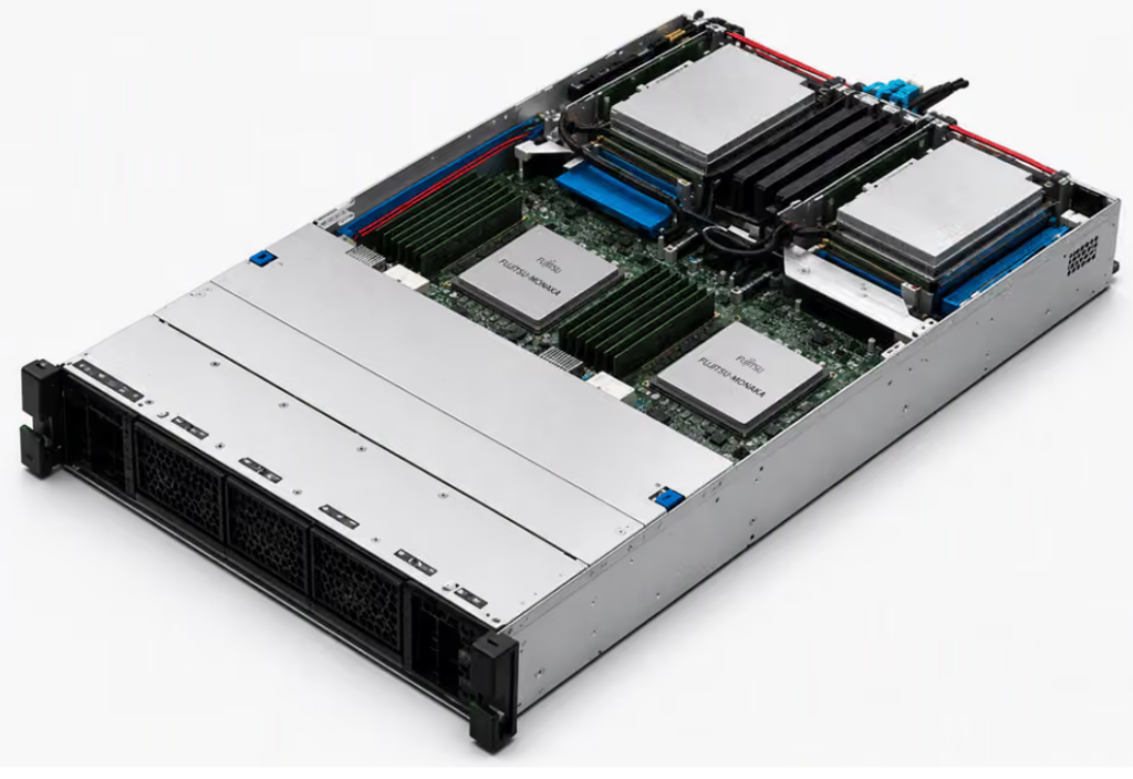
Fujitsu MONAKA Server 2U chassis with the lid off, showing two FUJITSU-MONAKA CPUs under their heatsinks, the DIMM banks around them, and the front drive bays

The processor itself uses a 3D-stacked design that combines CPU cores manufactured on a 2nm process with cache and I/O produced at 5nm. Fujitsu pairs the design with its ultra-low-voltage operation technology, which is where it says the power efficiency comes from.

Confidential computing is implemented at the hardware level through Arm CCA, encrypting applications and data while they are running in memory, including workloads operating in multi-tenant cloud environments.

MONAKA is also being developed for integration with accelerated platforms through Fujitsu’s work with NVIDIA to connect MONAKA CPUs and NVIDIA GPUs through NVLink Fusion.

MONAKA Server Keeps Development and Manufacturing in Japan

Sovereign infrastructure is the other major focus for MONAKA Server, with Fujitsu keeping the design, development, and manufacturing of the systems in Japan. Production will take place at the company’s Kasashima Plant, where component origins and manufacturing histories can be tracked through the production process.

That traceability takes the sovereign AI pitch down to the physical hardware, past the usual question of where data is stored or processed. Fujitsu is pairing the domestically produced hardware with its own AI software and management technologies for organizations that need greater control over their infrastructure, data, and supply chain.

The initial server lineup includes a 2U system with two MONAKA processors and 1U configurations with either one or two CPUs. Both air- and water-cooled deployments are supported, with the systems targeting AI inference and AI agent workloads.

Specification 2U Rackmount Model 1U Rackmount Model
Features All-in-one CPU/GPU/NW model optimized for existing DC/Edge environments Scalable model with flexible configuration and expansion according to environmental changes
Applications Digital Twin, Physical AI, Agentic AI, AI Inference Optimized for facility environments; flexible expansion from small to large scale
CPU Type / Quantity FUJITSU-MONAKA
2 CPUs
FUJITSU-MONAKA
1 to 2 CPUs
Base Frequency / Cores 2.1GHz × 144 cores 2.1GHz × 144 cores (air-cooled)
2.9GHz × 144 cores (liquid-cooled)
Memory Type / Slots RDIMM
24
RDIMM
12 (1-CPU configuration) / 24 (2-CPU configuration)
Storage Type / Slots E3.S SSD × 4
M.2 SSD × 2
E3.S SSD × 8
M.2 SSD × 2
Expansion Slots PCIe Gen6 (GPU support available) PCIe Gen6
Chassis Size 2U height 1U height
Cooling Method Air-cooled Air-cooled / Liquid-cooled


The 1U MONAKA Server also uses CDI/CXL technology to pool memory and accelerators, allowing those resources to be allocated across systems.

For academic and HPC environments, Fujitsu is preparing a 2U multi-node MONAKA Server with four nodes and two CPUs per node. The configuration is intended for computational workloads including surrogate models and fluid analysis.

Specification 2U Multi-node Model (4 nodes per chassis)
Features Multi-node model maximizing processing power within limited power and space
Applications AI data centers, large-scale simulations
CPU Type / Quantity FUJITSU-MONAKA
2 CPUs per node / 8 CPUs per chassis
Base Frequency / Cores 2.9GHz × 144 cores
Memory Type / Slots RDIMM
24 per node / 96 per chassis
Storage Type / Slots E1.S SSD × 2 per node
M.2 SSD × 2 per node
Expansion Slots PCIe Gen6
Chassis Size 2U height
Cooling Method Liquid-cooled

Fujitsu Connects MONAKA With Its AI Software

Fujitsu is extending the sovereign infrastructure approach into software through the Fujitsu Kozuchi AI platform, Takane enterprise generative AI, and industry-specific AI models. The combination brings together the processor, server hardware, AI platform, and generative AI software while supporting domestic data management, governance, traceability, security, and operational autonomy.

Future MONAKA hardware will include higher-density systems for AI data centers and rack-scale servers with autonomous operation features. Fujitsu is also developing robotic maintenance technology for future rack-scale systems, extending automation into physical server operations and maintenance.

Fujitsu’s math on the twice-the-throughput claim is that customers need half the servers and half the power for the same inference load, which is the figure the air-cooled pitch rests on. With no named comparison CPU or published benchmarks behind it, that’s the number to test when systems ship.

FUJITSU-MONAKA Availability

Standalone FUJITSU-MONAKA processors are scheduled to go on sale in November 2026, with availability planned for cloud and data center operators and server vendors in Japan, the US, APAC, and other markets during the fourth quarter of Fujitsu’s fiscal 2026.

Fujitsu also plans to begin sales of its 1U and 2U MONAKA Servers in Japan and Europe in November 2026 to data center operators, enterprises, academic and HPC buyers, and the defense sector. Select customers in the financial, telecommunications, and manufacturing sectors are expected to receive systems during the second half of fiscal 2026, with broader shipments in Japan and Europe scheduled to begin sequentially in April 2027.

FUJITSU-MONAKA

The post Fujitsu MONAKA Server Brings 2nm 144-Core CPUs to Air-Cooled AI Inference, On Sale in November appeared first on StorageReview.com.
FS Pairs 1.6T Scale-Out Optics With 500 km Coherent Modules and a Handheld Toolkit for AI Fabrics

FS has organized its AI optics into a two-part portfolio: Scale-Out transceivers at 400G, 800G, and 1.6T for the links inside a GPU cluster, and Scale-Across coherent modules at 400G and 800G for stitching clusters together across sites at distances up to 500 km. The Scale-Out side covers Ethernet, RoCE, and InfiniBand fabrics between GPU servers, NICs, switches, and racks; the Scale-Across side ships in OSFP and QSFP-DD for data center interconnect. Alongside both, FS is positioning the BOX 5 Ultra, a handheld toolkit for configuring, validating, and monitoring transceivers from 100M to 1.6T without a switch in the loop. The announcement is a packaging of parts FS has released one at a time since December, so the useful view is how they line up.

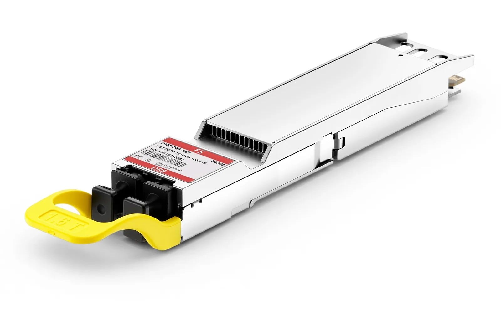
FS 1.6T OSFP DR8 optical transceiver with closed finned top heatsink, yellow pull tab, and dual MPO-12 ports (FS image)

1.6T at the Top of the Scale-Out Stack

The 1.6T parts are the OSFP-DR8-1.6T and OSFP-2FR4-1.6T, twin-port OSFP modules with a closed finned top that FS introduced for InfiniBand XDR networks. Both take 8x 200G PAM4 on the electrical side and run a Broadcom 3nm DSP. The DR8 uses silicon photonics with a CW laser, drives dual 4x 200G optical lanes at 1310nm over dual MTP/MPO-12 connectors, reaches 500 meters, and tops out at 25W; the 2FR4 uses EML transmitters and CWDM4 wavelengths over dual duplex LC, reaches 2 km, and draws up to 26W. FS says the modules are 100% verified on NVIDIA Quantum-X800 switches and lists NVIDIA part numbers (MMS4A00 and MMS4A50-XM) they’re built to match, with the DR8 aimed at 1.6T switch-to-switch links and 1.6T-to-two-800G breakouts into DGX B300 systems. That puts FS in the same 200G-per-lane generation the hyperscalers are buying into, whether through Qualcomm’s 1.6T interconnect deal with Amazon or the startup optics Lumilens is already shipping, at the compatible-module end of the market where FS competes on price and availability.

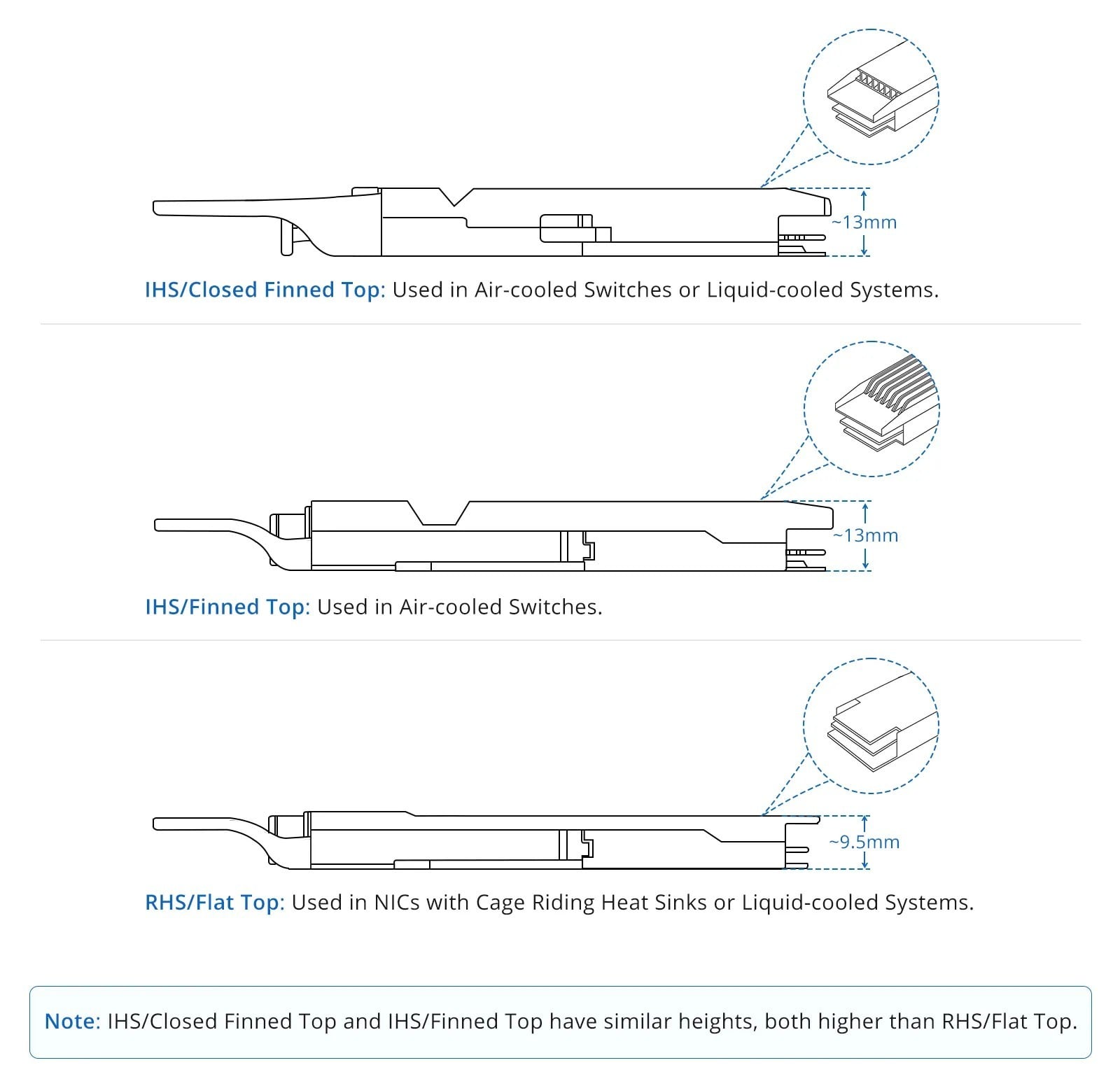
FS diagram comparing OSFP transceiver tops: IHS closed finned top and IHS finned top at about 13mm for air-cooled switches, and RHS flat top at about 9.5mm for NICs and liquid-cooled systems

The form factor detail matters more at 1.6T than it did at 400G. FS’s diagram shows the three OSFP tops it sells: the closed-finned top and the open-finned top both stand about 13mm and are meant for air-cooled switch cages (the closed version also works in liquid-cooled systems), while the flat top at roughly 9.5mm is for NICs with cage-riding heatsinks or liquid-cooled gear. The release says the 400G-to-1.6T lineup spans multiple form factors to match specific accelerator platforms, and that’s the choice it’s referring to: the same optics in the shape a given switch or NIC can cool.

800G Coherent for Scale-Across, and the Muxponder Behind It

The Scale-Across modules are the 800G ZR/ZR+ coherent optics FS launched in July, in OSFP and QSFP-DD, built on a Marvell 5nm DSP. FS rates them for 120 km and 500 km over single-mode fiber depending on the line, supports C-band and L-band operation to get more out of a fiber pair, and lists compliance with the OSFP and QSFP-DD MSAs plus 800ZR, OpenZR+, and OIF specifications, with Open FEC and CMIS/C-CMIS management. The 500 km figure in this week’s announcement is that July spec, restated with the caveat that reach depends on network configuration and optical line conditions.

For sites that aggregate client traffic before it reaches the line side, FS added the D7070 Series muxponder in August: a 1U box that takes 100GbE and 400GbE client services on QSFP28 and QSFP112 and puts them onto four 800G coherent wavelengths through CFP2-DCO line pluggables, for 3.2 Tb/s per platform, with WebGUI and CLI management for third-party NMS integration. “As AI and cloud workloads accelerate inter-site traffic growth, customers need DCI networks that can scale with demand while maximizing existing infrastructure,” said Bener Peng, product R&D manager at FS, when the D7070 launched.

BOX 5 Ultra: Provisioning Optics Without a Switch

The FS BOX 5 Ultra is the operations piece. It’s a portable transceiver toolkit that handles data rates from 100M to 1.6T across 15 form factors, OSFP, QSFP-DD, QSFP112, SFP-DD, and SFP among them, and FS says it works with modules from more than 200 brands. The functions are transceiver configuration, compatibility validation, module information reading, DDM monitoring, batch management, and wavelength tuning for tunable DWDM modules; the product page adds cloud batch coding, database access for easy config, and a 3,200mAh battery FS rates at up to 8 hours. The pitch is that a field tech can code, verify, and tune a tray of optics on a bench before any of them touch a production cage, which is the kind of work that otherwise eats switch ports and change windows.

FS hasn’t published module-level power or reach for every SKU in the 400G and 800G Scale-Out range in this announcement, and the 1.6T figures above come from the December launch of those specific parts. “The evolution from 800G to 1.6T is not only about higher speed but also about reshaping the optical interconnect architecture for AI,” said Kyrie Zhang, senior product manager at FS, at that launch, and the September portfolio is the company drawing the map around it.

FS AI Optical Transceivers

The post FS Pairs 1.6T Scale-Out Optics With 500 km Coherent Modules and a Handheld Toolkit for AI Fabrics appeared first on StorageReview.com.
Why Five EUC World Amplify 2026 Sponsors Are Betting on Milwaukee: 10ZiG, Nevona, Leostream, Nerdio, and Tassient

Two weeks from now (September 28 through October 1, opening with a reception on the 28th), we’ll be in Milwaukee, Wisconsin, for EUC World Amplify 2026. In a previous article, we shared why we’re excited to go. Building on that, we asked five EUC World Amplify 2026 sponsors, 10ZiG, Nevona.ai, Leostream, Nerdio, and Tassient, why they’re traveling to Milwaukee to back the event.

EUC World Amplify 2026 sponsors will gather at the Baird Conference Center in Milwaukee, Sept. 28 to Oct. 1, as shown on the event banner

Each company offered a different perspective on why it’s sponsoring and what it plans to show, but they all see Amplify as a chance to connect directly with EUC practitioners, trade real-world experiences, talk through the rapid changes reshaping the industry, and get honest feedback from the people working with EUC every day.

10ZiG Technology

“We’re attending and sponsoring EUC World Amplify because we believe some of the most valuable conversations in EUC happen when you bring together the people who actually design, deploy, and support these environments in one place. The EUC landscape is changing quickly, and IT Teams are having to navigate new challenges, such as vendor acquisitions, increased licensing costs, product end-of-life, security requirements, and evolving approaches to delivering apps, desktops, data, and digital workspaces, not forgetting the endpoints they are delivered on. Amplify creates an environment where those experiences can be shared openly and, technically, without everything becoming a sales pitch.

For 10ZiG, supporting that kind of community is important, as many new EUC friendships are formed in environments like this. We want to be part of the technical discussion, learn directly from the engineers dealing with these challenges every day, share what we’re seeing across different environments, and hopefully contribute some useful experiences of our own. That’s why we’re not just attending EUC World Amplify; we’re proud to be a Founding Sponsor and help support the EUC community behind it.”

Tom Dodds  – Global Strategic Alliances & Events Manager, 10ZiG Technology

Nevona.ai

“We come to Amplify for the people in the room who care about the same problems we do – the EUC work this audience fights every week, and that we lived ourselves for years at ControlUp: a Workspace client update that kills audio in a delivery group, a Citrix-to-AVD/LAS migration that stalls, FSLogix profiles bloating, a Patch Tuesday that breaks logon at 6am, GPO and baseline drift nobody has time to reconcile. That work doesn’t need another dashboard or another chat window. It needs something that can reach across the endpoint, the broker, AD, and Intune, find the root cause, and actually do the work.

Nevona is building autonomous agents that take that on end-to-end within your environment, not just the L1/L2 tickets. The migrations, the patch-and-regression recovery, the drift and identity cleanup, the standing engineering projects that never reach the top of the queue: the aim is an AI layer that operates IT the way your best engineers would, with the audit trail and guardrails to run unattended and safely. We’re here because this is the crowd that will tell us – bluntly – whether we got it right. Come find the team and put it to the test.”

Amir Harel – Co-founder & CEO, Nevona.ai

Leostream

“We are excited to sponsor an event driven by our peers and colleagues!

In the past, Leostream has been a bit of an outlier in the EUC market, but a lot has changed. Vendor consolidation, product changes, and shifting technology strategies have made flexibility and future-proofing more relevant than ever.

We’re looking forward to some interesting conversations and technical discussions at Amplify and the opportunity to showcase how our solution fits into this rapidly changing environment.”

Karen Gondoly – CEO, Leostream

Nerdio

“We’re living through the Great Migration in end-user computing, the largest replatforming this industry has seen since the shift from physical desktops to VDI. Organizations everywhere are moving off legacy VDI platforms and rethinking where their workloads should live: in the cloud, hybrid, on-premises, and, increasingly, in environments built for AI agents alongside human users.

I’ve spent my career building the platforms that underpin this shift, and I can tell you the hardest problems are solved by practitioners. We’re coming to Milwaukee to learn how this community of experts is navigating the shift as much as to share what we’re seeing, and the EUC community has always been generous with hard-earned knowledge. At a moment when nearly the entire market is rethinking its endpoint strategy, that collective knowledge is the most valuable asset this industry has.”

Scott Manchester – Chief Product and Technology Officer, Nerdio

Tassient

“As a disruptive new entrant in the EUC space, we are always looking for venues to present, demonstrate, and discuss our flagship product, Aipex, to a highly technical audience. After speaking with EUC practitioners who have attended previous Amplify events, we felt they were exactly the kind of audience we wanted to reach. Aipex is an AI-first remote monitoring, management, and remediation tool. In addition to a first-class set of human-driven troubleshooting tools, it allows IT administrators to use natural language with our Agentic AI Assistant to troubleshoot and, more importantly, remediate issues. We needed a place to connect with EUC administrators, and we felt that Amplify gave us exactly that.”

Jon Rolls – Founder and CEO, Tassient

We put Aipex through its paces earlier this year in our Tassient Aipex review.

Closing Thoughts

If you want to have technical discussions with fellow EUC practitioners and vendors, we highly recommend heading to Milwaukee and attending Amplify Sept. 28 to Oct. 1. We look forward to seeing you at the Baird Conference Center.

EUC World Amplify 2026

The post Why Five EUC World Amplify 2026 Sponsors Are Betting on Milwaukee: 10ZiG, Nevona, Leostream, Nerdio, and Tassient appeared first on StorageReview.com.
NASA-IBM Lunar Foundation Model Goes Open Source With a 2M-Tile Dataset and 22% Lower Ice-Mapping Error

IBM and NASA have released the NASA-IBM Lunar Foundation Model as open source, one of the first publicly available foundation models built for scientific study of the Moon. The weights, a technical report, and the machine-learning-ready dataset it was trained on are up on Hugging Face under the Prithvi family, which already covers Earth observation, weather, and heliophysics. The pitch is that decades of multi-instrument lunar data have outgrown hand-sifted maps and narrow, task-specific models, and a single pretrained backbone can be adapted to crater mapping, volcanic-feature detection, and ice prospecting without starting over each time. In IBM and NASA’s own benchmarks, the model cut root-mean-square error in flagging likely ice deposits by up to 22% against a SwinV2-B baseline.

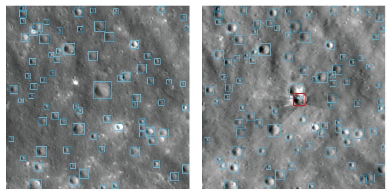
NASA-IBM Lunar Foundation Model crater detection output: two grayscale lunar surface tiles with blue bounding boxes drawn around detected craters

A TerraMind Backbone on 30 Layers From Nine Instruments

The model is built on a version of TerraMind, the Earth-observation model IBM developed with the European Space Agency, chosen for how it handles mixed data types and resolutions and learns cross-modal correlations that can fill in missing or noisy values. Fine-tuning for each lunar task uses low-rank adapters that keep 90% of the base weights frozen, which is what keeps the adaptation cost low. The training corpus is the part NASA says didn’t exist before: a unified, spatially aligned dataset of more than 30 layers from nine instruments across four missions, on the order of 2 million image tiles, with more than 1 million 1-meter camera images and close to 964,000 multispectral images at 100-meter resolution. Sources include imagery from NASA’s Lunar Reconnaissance Orbiter, gravity-field maps from the GRAIL mission at 20 kilometers per pixel, Lunar Prospector data, and complementary observations from JAXA’s SELENE/Kaguya. The benchmark collection, called SOMBench, ships alongside the model.

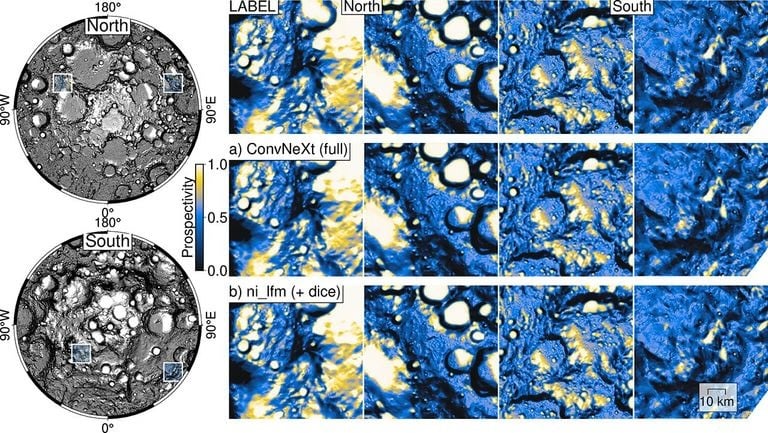
NASA-IBM Lunar Foundation Model ice prospectivity comparison: north and south polar maps beside label, ConvNeXt, and lunar foundation model prediction tiles on a blue-to-yellow prospectivity scale with a 10 km bar

Ice, Volcanic Patches, and Craters at Two Scales

The 22% figure comes from the ice task, where the model combines multimodal, multi-resolution observations to predict where ice may sit below the surface of permanently shadowed regions, the places a future Moon base would mine for water, oxygen, and rocket propellant. For volcanic history, it maps Irregular Mare Patches with 3% better coverage than SwinV2-B while training on imperfect labels, which IBM frames as comparable accuracy at lower fine-tuning cost. Crater detection splits by scale: at meter-scale resolution the model matches SwinV2-B, and at roughly 100-meter context scale it outperforms it by nearly 19% with half the training data. Michael Barker, the NASA lunar topography expert who co-led the project, said the payoff is in features whose ages are still contested: “The ages of these features remain a matter of great debate, so the more we can understand their distribution and properties, the better chance we have of resolving this mystery.”

“NASA has spent decades building an extraordinary scientific record of the Moon, but collecting data is only part of the job. We also have to make data easier for scientists to explore and use,” said Kevin Murphy, chief science data officer and acting chief data and AI officer at NASA Headquarters. Juan Bernabe-Moreno, director of IBM Research Europe, UK and Ireland, said the model “gives scientists a foundation to explore the Moon at scale, connecting observations across instruments, revealing patterns that are difficult to see in isolation, and providing an open platform the global research community can build on.”

Everything is available now under an open-source license, and IBM’s research blog walks through the three initial NASA use cases in more depth. It’s the same open-weights playbook IBM has run on the enterprise side with Granite 4.0, applied here to a science domain where the scarce resource is labeled data and the compute to fine-tune against it, and the immediate consumers are landing-site hazard analysis and resource prospecting for a sustained lunar presence.

NASA-IBM Lunar Foundation Model

The post NASA-IBM Lunar Foundation Model Goes Open Source With a 2M-Tile Dataset and 22% Lower Ice-Mapping Error appeared first on StorageReview.com.

Lightbits Inferra KV Cache Engine Claims 16x Session Density and 10M-Token Contexts

Lightbits Labs, the company that invented NVMe over TCP, is moving into inference software with Inferra, a KV cache orchestration engine that makes its public debut tomorrow, September 15, at the AI Infra Summit in Santa Clara. The software virtualizes GPU memory across DRAM and NVMe storage tiers and turns the KV cache into a persistent data layer, so attention states for long-context and multi-session workloads don’t have to fit in HBM or be recomputed when they fall out. Lightbits claims up to 16x more concurrent inference sessions on existing GPUs, a greater than 100x latency improvement from prefetching attention states in place of recomputing them, and context windows up to 10 million tokens, and says the engine has already run in customer beta programs, including one with OVH.

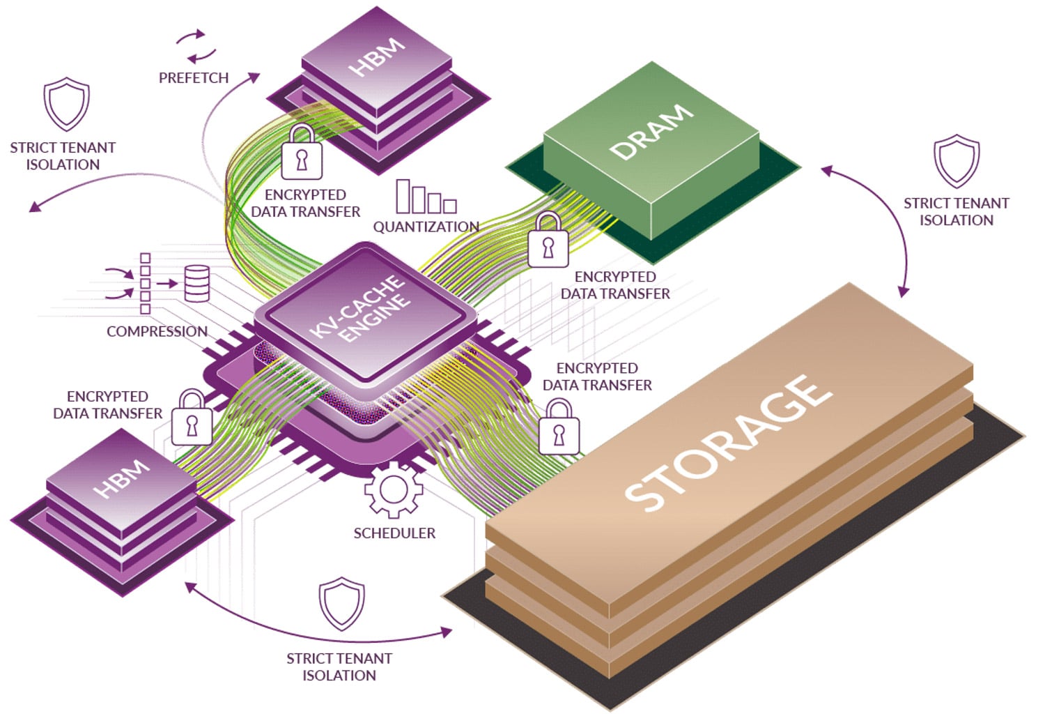
Lightbits Inferra architecture diagram with the KV cache engine sitting between GPU HBM, DRAM, and storage tiers, showing prefetch, compression, quantization, scheduling, encrypted transfer, and tenant isolation functions

Prefetch Instead of Recompute

The bottleneck Inferra targets is the one we walked through in our KV cache offload to flash piece: as context lengths grow and sessions multiply, the KV cache outgrows GPU memory, and the serving stack either evicts it and recomputes the prefill later or caps how many sessions a GPU can hold. Both paths burn GPU cycles on work that has already been done. Inferra keeps the cache alive across memory and storage tiers, and a predictive prefetcher pulls attention states back toward the GPU ahead of when the model needs them. Lightbits says that approach drives down both Time-to-First-Token (TTFT) and Time Per Output Token (TPOT), and the 100x figure it quotes is the latency improvement against recomputing those states from scratch.

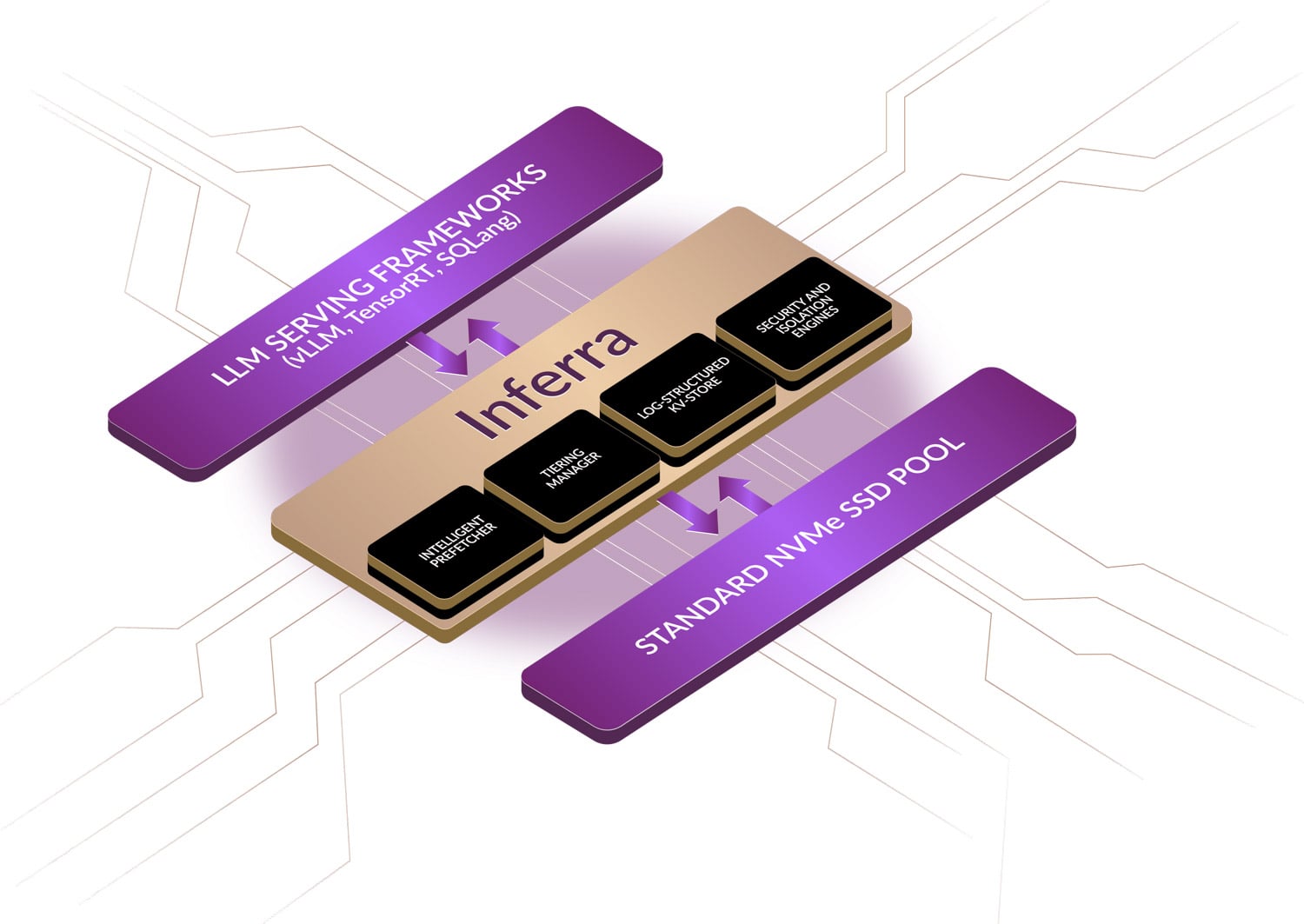
Lightbits Inferra block diagram showing its intelligent prefetcher, tiering manager, log-structured KV store, and security and isolation engines between LLM serving frameworks (vLLM, TensorRT, SGLang) and a standard NVMe SSD pool

Lightbits’ block diagram lays out the four pieces: an intelligent prefetcher, a tiering manager, a log-structured KV store, and security and isolation engines, sitting between the serving framework above and a standard NVMe SSD pool below. The company lists vLLM, TensorRT, and SGLang as supported serving frameworks and says the engine is GPU-and SSD-agnostic. The log-structured store is what makes a flash tier practical for a cache that changes constantly, since it appends updates sequentially and keeps small random writes off the drives, and we looked at how a 3 DWPD drive holds up in that role in our Solidigm D7-PS1030 review. On the multi-tenant side, Lightbits describes secure tenant isolation and intelligent cache management across shared inference infrastructure, with encrypted transfer between tiers, which is what lets a neocloud hand one KV pool to many customers with consistent SLAs.

Avigdor Willenz, co-founder and chairman of Lightbits Labs, framed the launch as a break from storage built for training pipelines. Inference “is a completely different paradigm,” he said, and “retrofitting legacy training and storage systems to solve the KV cache bottleneck simply doesn’t work. It was built for a different era. We engineered Inferra from the ground up specifically to solve the GPU efficiency problem, and it has already proven successful in customer beta programs.”

OVH, Solidigm, and the Booth 219 Demos

OVH is the named beta customer. “With Inferra’s intelligent KV cache tiering, we were able to demonstrate substantial GPU utilization gains, paving the way to providing our customers a more scalable and cost-effective foundation for their AI agent and RAG workloads,” said Yaniv Fdida, chief product and technology officer at OVH. Solidigm ran the engine in its AI Central Lab on D7-PS1010 drives, and Avi Shetty, the company’s VP of ecosystem, solutions, and market enablement, said the results “showcased how network-attached storage with intelligent software layer virtualization can break through the memory wall for large context, agentic AI.” That pairing of a network-attached NVMe pool with a software tier is Lightbits’ home turf; its LightOS block storage has been built on NVMe/TCP since 2019.

Ramesh Chettuvetty, senior vice president of AI product and business at Lightbits, called Inferra “the world’s first KV cache acceleration engine that eliminates idle GPUs and power context windows of up to 10M tokens on commodity hardware,” and said it “delivers instant payback and generates net positive savings from day one.” Those are vendor claims ahead of any independent testing, and the release doesn’t give pricing, packaging, or a general availability date; the engine is in customer beta today. Lightbits is running live demos of the session-density and latency results at Booth 219 during the summit, and has posted a Pod Efficiency Analyzer for teams that want to model the GPU savings against their own cluster before booking one.

Inferra by Lightbits

The post Lightbits Inferra KV Cache Engine Claims 16x Session Density and 10M-Token Contexts appeared first on StorageReview.com.

Second-Gen Single-Rack AWS Outposts Puts 2,688 vCPUs and 100TB of EBS in One 42U Rack

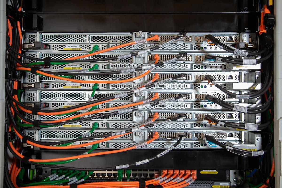
Top-down view of compute sleds in a single-rack AWS Outposts cabinet, each cabled with orange and black DACs to the switch below (AWS image) Top-down view of compute sleds in a single-rack AWS Outposts cabinet, each cabled with orange and black DACs to the switch below (AWS image)

AWS has made second-generation single-rack AWS Outposts generally available, a self-contained 42U rack that puts compute, storage, and networking together with up to 2,688 vCPUs and 100 TB of Amazon EBS. It runs the same APIs, console, automation, governance policies, and security controls as the multi-rack second-generation Outposts and the parent AWS Region, so an application built for the cloud moves on-premises without issue. AWS is suggesting this configuration is best for sites that need low latency, local data processing, or data residency but don’t have the floor space for a multi-rack deployment.

Rear of a single-rack AWS Outposts cabinet with fiber patching into a top-of-rack switch above a column of compute sleds (AWS image)

The Second Generation, Folded Into One Cabinet

AWS launched its second-generation Outposts racks in April 2025 as a multi-rack design that lets customers scale compute independently of a dedicated network rack. The single-rack version keeps that generation’s instances and networking and collapses them into a single 42U footprint, which is the point for customers who couldn’t justify or fit the multi-rack layout. Until now, the small end of the Outposts line was the 1U and 2U Outposts servers, which run on local instance storage and don’t offer EBS.

On the compute side, AWS supports the 7th-generation C7i, M7i, and R7i families on 4th Gen Intel Xeon Scalable processors, which the company says deliver twice the vCPU, memory, and network bandwidth of the first-generation racks and up to 40 percent better performance than the C5, M5, and R5 instances they replace, and AWS supports the newer 8th-generation C8i, M8i, and R8i families as well. EBS gp3 volumes have been available on second-generation racks since June 2025.

Accelerated Networking for Trading Floors and 5G Cores

The differentiator in the second generation is the pair of bare-metal accelerated networking instances. The bmn-sf2e instances pair Sapphire Rapids CPUs with AMD Solarflare X2522 network cards, in two sizes: bmn-sf2e.metal-16xl with 64 vCPUs, 512 GiB of DDR5, and two accelerated NICs at 100 Gbps, and bmn-sf2e.metal-32xl with 128 vCPUs, 1,024 GiB, and four accelerated NICs at 200 Gbps. AWS built them for capital markets, with native Layer 2 multicast, precision time protocol, and equal cable lengths so firms can meet fair-trading and equal-access rules on premises while plugging into existing trading infrastructure.

The bmn-cx2.metal-48xl carries 192 vCPUs, 1,024 GiB of DDR5, and two NVIDIA ConnectX-7 400G NICs for 800 Gbps aggregate, with the same L2 multicast and hardware PTP support, targeted toward real-time market data distribution, risk analytics, and telecom 5G core workloads. A third family, bmn-cx3a, appears in the single-rack instance list without a published spec.

Top-down view of compute sleds in a single-rack AWS Outposts cabinet, each cabled with orange and black DACs to the switch below (AWS image)

Availability

Single-rack second-generation Outposts can be ordered now from the AWS Outposts console, with the list of supported countries and territories on the Outposts rack FAQ page. The storage ecosystem that grew up around the first generation carries over: Dell’s PowerStore and Pure’s FlashArray are both validated as external block storage for Outposts, which matters for sites that outgrow the 100 TB of EBS inside the rack.

AWS Outposts Rack

The post Second-Gen Single-Rack AWS Outposts Puts 2,688 vCPUs and 100TB of EBS in One 42U Rack appeared first on StorageReview.com.
LTM Builds a Lightwell Remediation Services Practice Around IBM and Red Hat’s $5B Open-Source Program

IBM and Red Hat Project Lightwell graphic IBM and Red Hat Project Lightwell graphic

LTM, the Larsen & Toubro Group services company that was LTIMindtree until its February rebrand, is building a Lightwell remediation services practice around the $5 billion IBM and Red Hat program for securing open-source software with AI-generated, vendor-validated fixes. IBM’s clearinghouse produces validated, production-ready patches for open-source dependencies; LTM’s job is getting them into customer environments. The company says its planned portfolio spans remediation strategy, dependency analysis, risk-based prioritization, remediation program management, DevSecOps integration, testing and validation, and large-scale deployment support.

IBM and Red Hat Lightwell key art with blue data streams converging on a central patch symbol, the program LTM is now building Lightwell remediation services around

Where LTM Fits in the Lightwell Model

Lightwell’s premise, as IBM and Red Hat laid it out in May, is that AI is accelerating vulnerability discovery faster than enterprises can remediate, so a clearinghouse staffed by more than 20,000 engineers ingests vulnerability data from live deployments, validates fixes, and ships them as production-ready patches through subscription services. In July, the two companies added a Lightwell Network tier, which is generally available with a library of remediations spanning current and legacy libraries, and a Lightwell Clearinghouse Premier tier in limited-availability commercial onboarding, and named a bench of deployment partners that included LTM alongside Accenture, Deloitte, HCLTech, Infosys, Kyndryl, TCS, and others. This week’s announcement turns LTM’s spot on that list into a defined offering, backed by its standing as an IBM Platinum Partner.

“As AI accelerates software development and vulnerability discovery, enterprises need a faster and more scalable approach to remediation,” said Chandan Pani, chief information security officer at LTM. “Lightwell represents a significant advancement in securing the open-source software supply chain by bringing AI-driven remediation and trusted software maintenance into the enterprise. Through our collaboration with IBM, LTM will help organisations strengthen their cyber resilience at scale.” Sandip Patel, managing director of IBM India and South Asia, framed it as collective defense: “As AI accelerates vulnerability discovery, collaboration across the ecosystem becomes increasingly important. Bringing LTM’s engineering and transformation expertise to Lightwell can help enterprises mitigate risk and build more resilient software supply chains.”

Why IBM and Red Hat Want the Integrators

Red Hat’s Ryan King, vice president of AI and infrastructure partners, was the most direct about why the program needs a partner channel at all: “AI-driven discovery has pressed the demand for speed and patch delivery far beyond the means of any one single vendor.” A validated patch from the clearinghouse still has to be prioritized against a customer’s actual dependency graph, tested in that customer’s pipelines, and rolled out across an estate without taking down the applications it protects, and that’s the work LTM says it’ll take on, with the stated goal of heading off zero-day exploits and production downtime.

LTM describes the portfolio as planned, and the release carries no pricing, availability dates, or named customers, so this is a go-to-market announcement for services that are being built around Lightwell’s existing tiers. What it does signal is that Lightwell’s financial-services early adopters, which included Bank of America, Citi, Goldman Sachs, JPMorganChase, and Visa at launch, will be followed by a wider enterprise base that reaches the program through integrators like LTM, and we’ll be watching for the first deployment specifics.

IBM Lightwell

The post LTM Builds a Lightwell Remediation Services Practice Around IBM and Red Hat’s $5B Open-Source Program appeared first on StorageReview.com.
IBM Quantum System Two Heads to Switzerland: 120-Qubit Nighthawk r2 at CSCS by End of 2026

IBM Quantum System Two in IBM's Poughkeepsie quantum data center, with its mirrored hexagonal enclosure beside cooling manifolds and rows of black compute racks IBM Quantum System Two in IBM's Poughkeepsie quantum data center, with its mirrored hexagonal enclosure beside cooling manifolds and rows of black compute racks

IBM and Lockheed Martin are setting up a quantum innovation hub at ETH Zurich, and its core is Switzerland’s first IBM Quantum System Two, to be installed at the Swiss National Supercomputing Centre (CSCS) in Lugano by the end of 2026. The hub comes out of an offset agreement with armasuisse, Switzerland’s Federal Office for Defence Procurement. IBM will operate the machine, which runs on an IBM Quantum Nighthawk processor, while ETH Zurich supplies the expertise and coordinates access for Swiss universities, startups, and companies.

IBM Quantum System Two in IBM's Poughkeepsie quantum data center, with its mirrored hexagonal enclosure beside cooling manifolds and rows of black compute racks

A 120-Qubit Nighthawk r2 Next to Alps

The Swiss system will run IBM’s Nighthawk r2, which IBM calls the fastest and most advanced processor it has made available to users. It carries 120 programmable qubits and a new high-speed qubit reset architecture that lets it execute more than 100,000 circuits per second, which IBM puts at up to 25x the circuit throughput of the Heron processors it succeeds. IBM also says the part has already demonstrated accurate computations on quantum circuits containing 7,500 gates. Nighthawk is the processor family IBM has been building its near-term roadmap around, most recently when it linked two cryogenic modules below 15 millikelvin on the way to its 2029 fault-tolerant machine.

CSCS will house the System Two in the same facility as its Alps supercomputer and provide the power, cooling, and security, so the quantum node sits directly alongside national HPC infrastructure for the chemistry, materials science, optimization, and financial services work the hub is targeting. That’s the same quantum-centric supercomputing pattern IBM has been describing with partners like AMD, where a quantum processor handles the parts of a problem classical hardware can’t simulate efficiently, and the supercomputer handles the rest. The IBM and ETH Zurich agreement to install and operate the system runs for an initial three years, through 2029. Until the hardware arrives, organizations joining through ETH Zurich get access to IBM’s cloud-based quantum fleet, and the whole arrangement builds on a 10-year collaboration between IBM and ETH Zurich on the next generation of algorithms for AI and quantum computing.

Lockheed Martin’s Two Projects and the Training Pipeline

The hub formalizes two joint projects between IBM and Lockheed Martin: quantum sensing for navigation, and quantum simulation aimed at improving the additive manufacturing of metallic alloys. “This project extends the strategic relationship between Lockheed Martin and IBM in quantum and AI while positioning Switzerland as a leader in these critical, cutting-edge fields,” said Dr. Craig Martell, vice president and chief technology officer at Lockheed Martin. Alessandro Curioni, vice president of algorithms and applications at IBM Research and director of the Zurich Research Laboratory, said the goal is “to put world-class quantum hardware, software and expertise directly into the hands of Switzerland’s thriving academic institutions and industries.”

“Switzerland will gain access to essential research infrastructure that will enable us to further advance the exploration of this emerging technology,” said ETH Zurich President Joël Mesot. Alongside the hardware, the Swiss ecosystem gets IBM Quantum Network and IBM Quantum Platform learning offerings, including coursework, certifications, and workshops, plus support for hackathons, conferences, and partner forums. IBM’s Starling roadmap puts a fault-tolerant system in Poughkeepsie by 2029, and installations like the one at CSCS are where the algorithms for that machine get worked out on utility-scale hardware in the meantime.

IBM Quantum Hardware

The post IBM Quantum System Two Heads to Switzerland: 120-Qubit Nighthawk r2 at CSCS by End of 2026 appeared first on StorageReview.com.
Palantir and NVIDIA Deploy a Sovereign Nemotron Supply Chain Stack, Starting With the 1.3 Million Parts in Every Vera Rubin Rack

Palantir and NVIDIA logos side by side on a black background Palantir and NVIDIA logos side by side on a black background

Palantir and NVIDIA have built a sovereign AI stack for supply chain operations and are running it first inside NVIDIA’s own supply chain, the one that has to line up 1.3 million parts for every Vera Rubin rack. The stack brings NVIDIA Nemotron open models into Palantir Foundry and its Artificial Intelligence Platform (AIP), grounded in the Palantir Ontology, with the aim of giving planners visibility across the chain, surfacing constraints early, and codifying the operational judgment that, to this point, lives in people’s heads. NVIDIA’s deployment starts with materials allocation, the decisions about which parts go where that set how fast a rack moves from wafer to first token.

Palantir and NVIDIA logos side by side on a black background

NVIDIA’s Supply Chain as the First Customer

A rack-scale AI system needs compute, memory, networking, power, cooling, and mechanical parts to arrive together, across thousands of suppliers and a global manufacturing network, and NVIDIA says the Vera Rubin supply chain is twice the size of Grace Blackwell’s. The new stack gives NVIDIA’s supply chain teams what the companies call a shared command center, beginning with allocation decisions, so they can identify constraints earlier, evaluate alternatives faster, and allocate materials based on end-to-end production impact.

“Supply chains are the operating system of the physical economy, and AI factories are among the most complex systems ever built,” said Jensen Huang, founder and CEO of NVIDIA. “From wafers and components to manufacturing, systems and customer delivery, hundreds of companies and trillions of dollars of global economic activity come together to deliver AI infrastructure.” Palantir cofounder and CEO Alex Karp put it more bluntly: “NVIDIA has arguably the most valuable, intricate and complex supply chain in the world.” The two companies first announced their operational AI work together at GTC DC last October; this is that partnership producing a deployed system.

Post-Trained Nemotron, cuOpt, and a Human in the Loop

Palantir customers post-train Nemotron open models on their own operational data inside Foundry and AIP, using NVIDIA NeMo Data Libraries to prepare and augment it. Within AIP, NVIDIA cuOpt handles optimization and scenario planning, so teams can model supply constraints, weigh tradeoffs, and see the operational impact of an allocation decision before making it. The post-trained model recommends actions, explains the tradeoffs, and flags emerging risks, while the supply chain experts keep the final call. Palantir Autopilot, integrated with the NeMo AutoModel and NeMo RL libraries, closes the loop by feeding each recommendation, planner action, and production outcome back into model improvement, which is how the companies say operational knowledge gets preserved instead of lost when people move on.

NVIDIA’s technical write-up of its own deployment gives a sense of how light the model work is. The production model is Nemotron 3.5 Lightning, a 30-billion-parameter mixture-of-experts model with roughly 3 billion parameters active per pass, chosen over the larger Nemotron 3 Ultra for agentic workflows. Post-training used LoRA adapters with the base weights frozen and finished on two B200 GPUs in minutes. On NVIDIA’s internal allocation-decision benchmark, the post-trained Lightning model scored 86.7 percent accuracy, 31.2 points ahead of the untuned Nemotron 3 Ultra and 69.2 points ahead of its own base weights. Those are NVIDIA’s numbers on NVIDIA’s data, but they make the case for the approach: a small open model with the organization’s own decisions trained into it beats a much larger general one on that organization’s problem.

Sovereign by Design

Because the data is NVIDIA’s supply chain, the deployment runs on NVIDIA reference architectures and the jointly developed Palantir Sovereign AI Operating System Reference Architecture, or SAIOS, which Dell Technologies and Cisco support. Proprietary data, model weights, and inference stay inside a single governed environment, and the stack can be deployed on premises with Cisco or Dell, or in colocation and cloud with Rackspace and Nebius. Palantir and NVIDIA say they intend to extend what they learn from NVIDIA’s deployment to customers in agriculture, manufacturing, pharmaceuticals, retail, energy, healthcare, automotive, aerospace, and government, and will show the stack and its industry applications at Palantir’s AIPCon 11.

Palantir AIP

NVIDIA Nemotron

The post Palantir and NVIDIA Deploy a Sovereign Nemotron Supply Chain Stack, Starting With the 1.3 Million Parts in Every Vera Rubin Rack appeared first on StorageReview.com.
Backblaze B2 and WEKA NeuralMesh Validated as a Two-Tier AI Storage Pipeline, With Snap-to-Object Checkpoints in B2

WEKA and Backblaze logos side by side on a dark red and purple gradient background WEKA and Backblaze logos side by side on a dark red and purple gradient background

Backblaze and WEKA have validated their two platforms together for AI pipelines, pairing WEKA NeuralMesh as the performance tier that feeds GPUs with Backblaze B2 Cloud Storage as the capacity tier that holds everything else. The integration, sizing, tuning, and testing are already done, so an AI infrastructure team can deploy a proven two-tier layout without building and qualifying its own. Certification of B2 for NeuralMesh is underway, and both companies say customers can contact either one to get started now.

WEKA and Backblaze logos side by side on a dark red and purple gradient background

Two Tiers, One Data Lifecycle

Raw, unstructured data, meaning the training sets, media libraries, and source files, lives in B2. When a dataset becomes part of a performance-sensitive job, it’s made available to NeuralMesh and served to the accelerators from there. Once a checkpoint, an output, or any other asset no longer needs high-performance access, it goes back to B2, where it can be reused in a later run or pulled back if a job has to recover to an earlier stage. The companies frame it as speed where the GPUs are and capacity everywhere else, with the data moving between the two as its access pattern changes.

“AI teams need their GPUs fed and an infrastructure with the performance and capacity to support the full AI data workflow. WEKA has mastered the performance tier. We’ve spent nearly two decades doing the same for capacity storage,” said Gleb Budman, CEO of Backblaze. Nilesh Patel, Chief Strategy Officer at WEKA, described the same pressure from the other direction: “AI workloads are stretching storage in two directions at once. GPUs need microsecond access to data to stay fed, while datasets and checkpoints are growing to exabyte scale. Our collaboration with Backblaze gives customers a validated path to both, without the cost of building and testing that integration themselves.”

Snap-to-Object Tested Against B2

Another interesting piece is NeuralMesh’s Snap-to-Object, which the companies say they’ve tested with Backblaze. Snap-to-Object writes a consistent snapshot of a NeuralMesh file system out to an object store, and with B2 as the target, that store is the same capacity tier the raw data and retired checkpoints already end up in. For a training run, that means a team can revert to a checkpoint or recover saved inference data from B2 without improvising a fix in the middle of the job, and without maintaining a separate destination for snapshots. The economic effect is a cloud object tier behind NeuralMesh that’s priced as capacity, holding the snapshots alongside the data they protect.

Backblaze has been positioning B2 as the capacity layer for AI throughout the year, from the B2 Neo offering for neocloud platforms to its performance benchmarking program, and WEKA gives it a performance-tier partner on the GPU side of that.

Backblaze B2 Cloud Storage

WEKA NeuralMesh

The post Backblaze B2 and WEKA NeuralMesh Validated as a Two-Tier AI Storage Pipeline, With Snap-to-Object Checkpoints in B2 appeared first on StorageReview.com.
Scality Maestro 1.1 Manages ARTESCA Fleets From One Console With No VPN Into Customer Sites

Scality Maestro dashboard listing 114 ARTESCA deployments with 12.15PiB of managed data, fleet health showing nine deployments unhealthy, and per-cluster node counts, capacity, and ARTESCA version Scality Maestro dashboard listing 114 ARTESCA deployments with 12.15PiB of managed data, fleet health showing nine deployments unhealthy, and per-cluster node counts, capacity, and ARTESCA version

Scality has made Maestro 1.1 generally available, a fleet management platform for service providers running large numbers of Scality ARTESCA object storage deployments on behalf of their customers. The target is the backup-as-a-service business that starts as a handful of ARTESCA clusters and grows to tens or hundreds, each sitting inside a different customer’s network and each needing monitoring, software and firmware updates, and capacity tracking for the monthly bill. Maestro puts all of that behind one console, with no VPN tunnel into any customer site.

Scality Maestro dashboard listing 114 ARTESCA deployments with 12.15PiB of managed data, fleet health showing nine deployments unhealthy, and per-cluster node counts, capacity, and ARTESCA version

What Scality Maestro Manages

Scality says it co-developed Maestro with its cloud and service provider partners and that it’s already in production. Fleet-wide health monitoring and alerting shows every ARTESCA deployment from a single view. Lifecycle management reaches down to the hardware, so ARTESCA software upgrades and server firmware updates can be pushed across the whole fleet at once. Capacity utilization is aggregated across all customer sites and fed into automated pay-as-you-go billing, which replaces the end-of-month reports assembled by hand. The screenshot Scality supplied shows the scale it’s built for: 114 deployments, 12.15PiB under management, and an “upgrade all” control for the clusters that have fallen behind the current ARTESCA release.

“Service providers building BaaS businesses on Scality ARTESCA are managing infrastructure at a scale that demands enterprise-grade operational tooling,” said Thomas Danan, Sr. Product Director at Scality. “Maestro was built with our SCSP partners to solve the real operational problems they face every day with centralized visibility, automated management, and the billing infrastructure to run a sustainable managed service. The fact that it requires no VPN and no network reconfiguration on the customer side was a hard requirement from day one.”

Outbound Only: How the No-VPN Model Works

The design choice Danan is describing is worth understanding. Managing infrastructure you don’t own usually means opening a tunnel into every customer environment, with the network reconfiguration and standing access that implies. Maestro inverts the connection: each ARTESCA deployment opens a connection out to Maestro and reports in, and Maestro never reaches back into the customer network. That single rule removes the VPN requirement and the customer-side firewall work, and it’s why the platform can scale from dozens of sites to hundreds without each new customer becoming a network project.

ARTESCA external connections screen showing the cluster endpoint, an Add Maestro connection button, and two Maestro connections, one linked and active and one in error

Autodata, which runs ARTESCA deployments across customer sites in the UK and Ireland for its backup service, is one of the early users. Before Maestro, CEO Dominic McLoughlin said, every one of those deployments was “independently managed, with separate logins, VPN tunnels, manual update cycles, and monthly capacity reports assembled by hand. Instead, Maestro gives us a single view of the entire fleet. Software updates that consume hours of staff time can now be monitored centrally, and we can grow the fleet without adding operational headcount.”

Although it was designed for the service provider market, Scality says Maestro fits enterprises that run ARTESCA across branch offices, edge locations, or as part of a distributed data protection architecture, where the same inflection point arrives once deployments grow past a handful of sites. Maestro 1.1 is available now as an on-premises deployment and supports all ARTESCA installations running version 4.0.3 or later. A SaaS delivery model is planned for a future release, and documentation is available to Scality service providers through the partner portal.

Scality Maestro

The post Scality Maestro 1.1 Manages ARTESCA Fleets From One Console With No VPN Into Customer Sites appeared first on StorageReview.com.
d-Matrix Raptor XPUs Join NVIDIA MGX Racks Through NVLink Fusion, With First Systems Due Q4 2027

NVIDIA rendering of a d-Matrix Raptor compute tray with NVLink Fusion, an NVIDIA NVLink switch tray, and the full d-Matrix MGX rack NVIDIA rendering of a d-Matrix Raptor compute tray with NVLink Fusion, an NVIDIA NVLink switch tray, and the full d-Matrix MGX rack

d-Matrix will put its next-generation Raptor inference XPUs into NVIDIA’s MGX rack architecture using NVLink Fusion, under a collaboration with NVIDIA that the company describes as a multi-year product roadmap. The first product is a d-Matrix rack built on the MGX reference design with NVIDIA Vera CPUs, NVLink switches, BlueField-4 DPUs, ConnectX-9 SuperNICs, and Spectrum-X Ethernet, aimed at AI labs, hyperscalers, and neoclouds selling what d-Matrix calls premium, ultra-low-latency token services. Initial availability of Raptor XPUs in the MGX rack is expected in the fourth quarter of 2027.

NVIDIA rendering of a d-Matrix Raptor compute tray with NVLink Fusion, an NVIDIA NVLink switch tray, and the full d-Matrix MGX rack

What NVLink Fusion Gives d-Matrix

The argument for the deal is centered around time and risk. Getting a custom accelerator into production at AI factory scale means sourcing and validating a scale-up interconnect, a rack design, power delivery, liquid cooling, scale-out networking, and a supply chain. NVLink Fusion is NVIDIA’s program for letting third-party XPU and CPU designers plug into a stack NVIDIA has already built. For d-Matrix, that means Raptor gets the same NVLink scale-up domain, MGX rack, cooling, and supply chain that NVIDIA’s own systems use, and data center operators can stand up one-rack architecture that carries GPUs, CPUs, and XPUs.

“Demand for inference is soaring, but capital, time and energy remain finite,” said Sid Sheth, cofounder and CEO of d-Matrix. “With NVLink Fusion and MGX, we can integrate our Raptor XPUs into a broadly deployed, liquid-cooled architecture, giving customers a faster, lower-risk path to deploy and scale ultralow-latency inference.” NVIDIA CEO Jensen Huang framed it from the other side: “With NVIDIA AI infrastructure deployed across cloud and on-premises data centers worldwide, NVLink Fusion gives partners like d-Matrix a path to integrate seamlessly with NVIDIA compute platforms, expanding accelerator choice for customers building the next generation of AI factories.”

The interconnect itself is sixth-generation NVLink, which NVIDIA rates at 3.6TB/s per GPU or XPU and 260TB/s of aggregate bandwidth across a 72-accelerator all-to-all domain, more than 14 times the bandwidth of PCIe Gen6 by NVIDIA’s comparison. d-Matrix plans to use it to connect Raptor XPUs into a single high-bandwidth scale-up domain, with the racks built from modular, cable-free MGX trays. Astera Labs is also part of the design, supplying connectivity for the system as an existing member of the NVLink Fusion ecosystem, which also includes Arm, Intel, Fujitsu, SiFive, Marvell, MediaTek, Samsung, Alchip, GUC, Cadence, Synopsys, Ayar Labs, and Lightmatter. We covered MediaTek’s NVLink Fusion XPU work and AWS bringing NVLink Fusion to Trainium in the last two weeks; d-Matrix is the latest to take the same route.

Disaggregated Inference: GPUs for Prefill, Raptor for Decode

d-Matrix is pitching what it calls heterogeneous disaggregation, where a Raptor rack sits alongside a Vera Rubin NVL72 and takes the phase of inference it’s built for. For AI coding assistants, the example d-Matrix uses, the GPUs handle the compute-heavy prefill phase while the Raptor XPUs run the latency-sensitive decode phase, where interactivity is what the customer is paying for. The same split applies to real-time chatbots and voice agents, and it’s why d-Matrix keeps describing the target as a premium token economy: workloads where buyers pay more for speed.

Raptor is the follow-on to d-Matrix’s Corsair XPU, which is in production today. It extends the company’s memory-centric design with what d-Matrix calls a first-of-its-kind 3D DRAM stacking approach, pairing a DRAM chip with an SRAM compute chip in a single two-story package. Co-founder and CTO Sudeep Bhoja previewed the technology at Hot Chips 2026, and the technical details have been published through IEEE. d-Matrix says Raptor was designed from the start for NVLink Fusion and MGX integration, is expected to tape out before the end of this year, is under evaluation at hyperscalers and frontier labs, and is backed by more than 100 patents. The company is demonstrating the design at the AI Infra Summit next week.

d-Matrix

The post d-Matrix Raptor XPUs Join NVIDIA MGX Racks Through NVLink Fusion, With First Systems Due Q4 2027 appeared first on StorageReview.com.

Eaton HDXL Rack PDU Review: 81kW From a Single Zero-U PDU for AI Racks

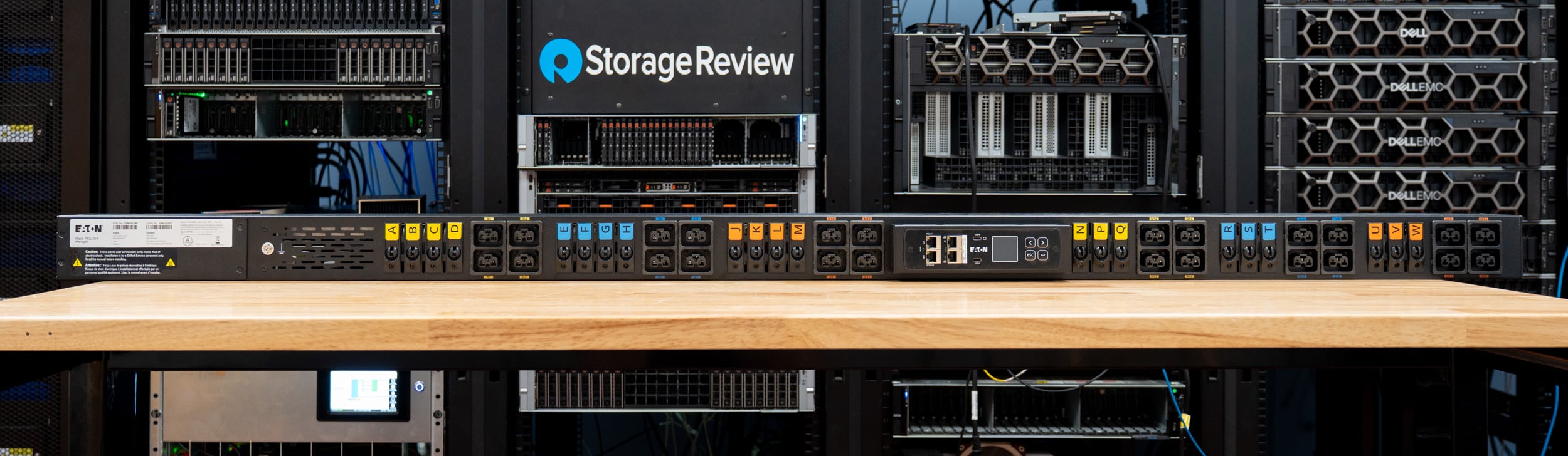
Eaton HDXL Rack PDU mounted vertically in a rack, with lettered C39 outlets feeding server power cords Eaton HDXL Rack PDU mounted vertically in a rack, with lettered C39 outlets feeding server power cords

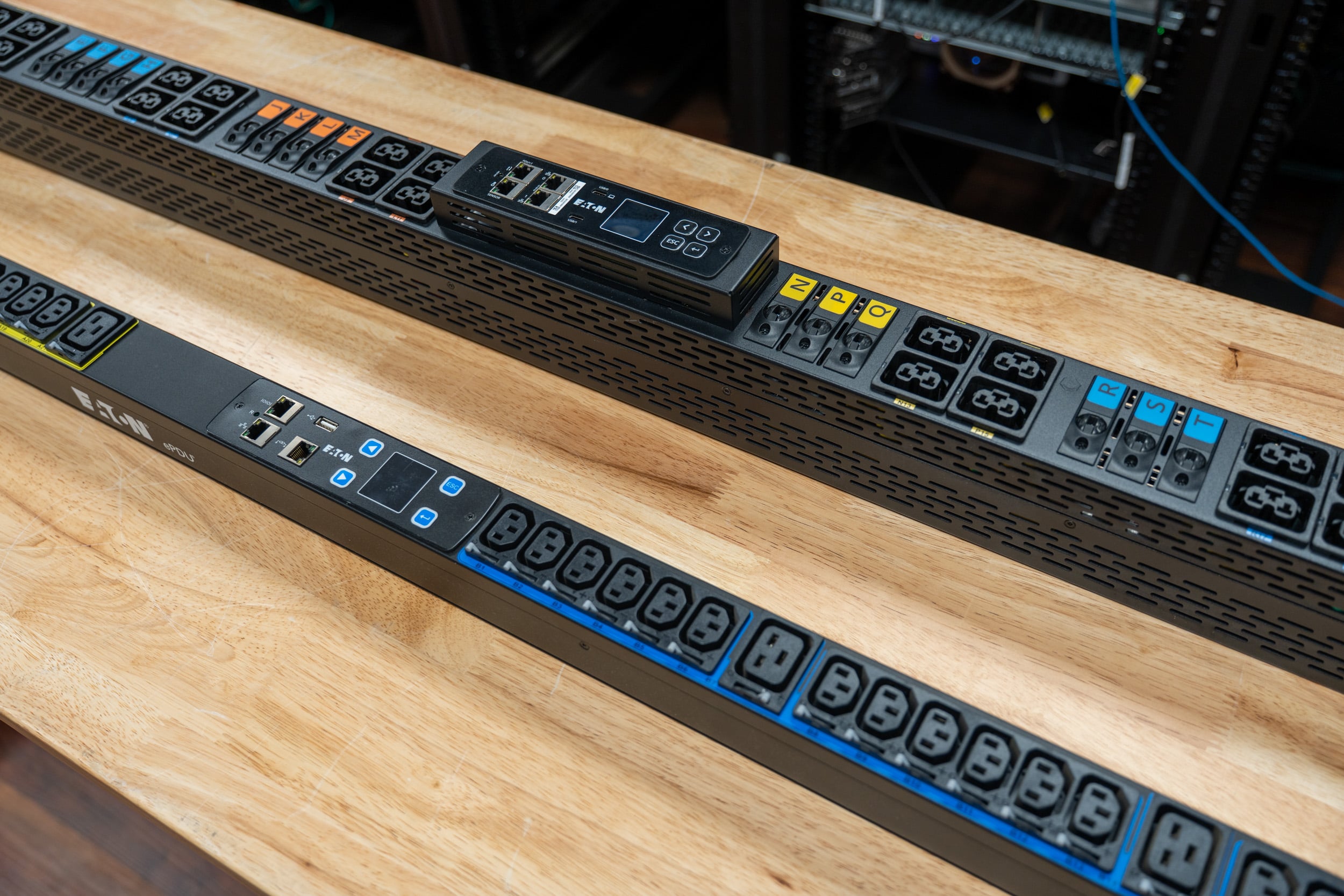
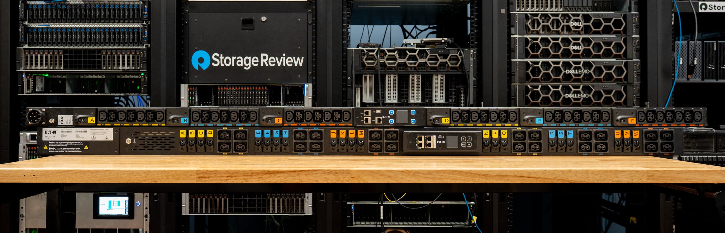
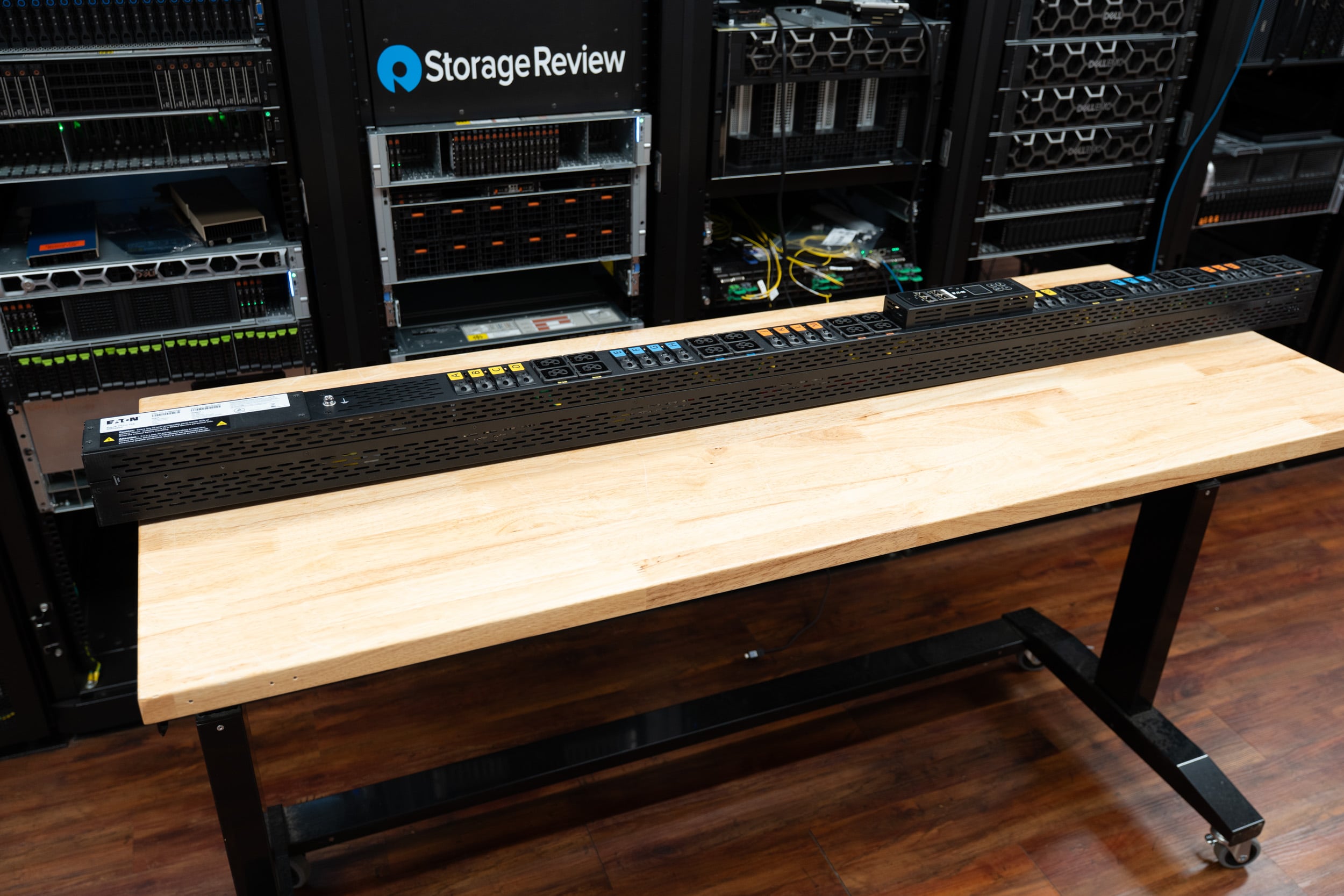
Eaton is getting ready to ship the kind of PDU that didn’t need to exist five years ago. The HDXL Rack PDU G4, arriving in the fourth quarter of 2026, delivers 56-81kW from a single zero-U unit, with 24 outlets, 21 branch breakers, and a 100A corded or 140A terminal-block input. Four models launch in the second half of the year as standard offerings. Eaton sent us two units, and while our lab doesn’t have the 480V high-voltage three-phase service these are built for, the conversation right now is why PDUs in this class suddenly matter and what changed between this and the G3 platform we reviewed in 2023.

The Power Problem Dense AI Racks Created

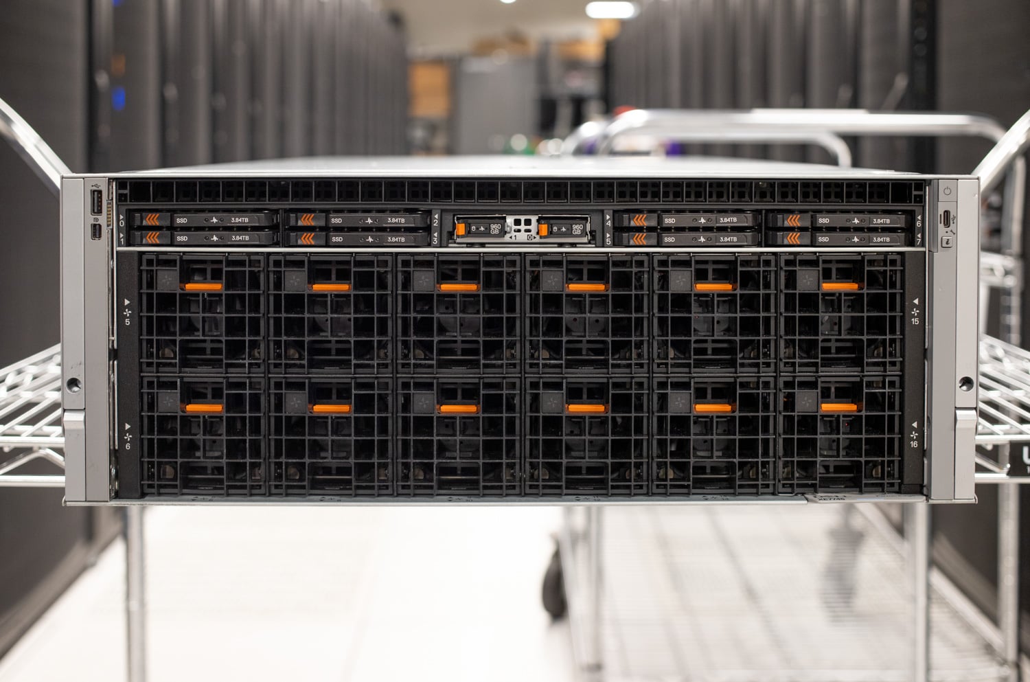
The electrical math that justifies an 81kW PDU starts with a GPU single server. Dell’s PowerEdge XE7745, the 4U air-cooled GPU box we have covered extensively in our work with Oregon State, carries dual 5th-gen AMD EPYC processors and up to eight double-wide 600W PCIe accelerators, such as the NVIDIA RTX PRO 6000 Blackwell Server Edition, NVIDIA’s H200 NVL, or AMD’s Instinct MI350P. Dell feeds that with up to eight 3200W power supplies per chassis, split across two power zones: two for the server sled and six for the GPUs, and its configuration matrix disqualifies the smaller 2400W supply once eight 600W cards are involved. That’s up to 25.6kW of supply capacity, and eight power cords per 4U server, with 277 VAC and HVDC supply variants tailored to the exact class of high-voltage feeds the HDXL is designed to distribute. The Xeon 6-based XE7740 sibling matches the same eight-PSU, two-zone design. Run N+N redundancy across A/B feeds, and each server presents four cords per side; six of them consume all 24 outlets on each of a pair of HDXLs.

Dell PowerEdge XE7745 front view in the StorageReview lab showing the 4U fan wall and NVMe bays

Stack those in a rack, and the power consumption and distribution get significant fast. Six XE7745-class systems consume 24U and, fully populated, 48 power cords: 24 per feed, which is precisely the outlet count of one HDXL per side. Accelerator load alone on those six systems runs 28.8kW before the CPUs, fans, memory, and storage do anything. Six systems are the outlet ceiling: 24 cords per feed against 24 C39 positions. Six systems’ worth of feed-side PSU capacity is 76.8kW, sitting just inside the 81kW model’s rating, so on the top HDXL, the electrical limit and the outlet limit converge on the same rack. The 56kW model carries the same six systems against realistic draw, with less margin for a single-feed failover event. Either way, this is exactly the “assuming you have enough power to the rack” scenario: the building feed, not the distribution, becomes the constraint, which is a common problem to have in 2026.

The alternative is what dense deployments do today: gang multiple mid-capacity PDUs per rack. Our Eaton G3 Universal PDU review unit topped out at 23kVA with its largest input cord, designed more for switches, storage hardware, and general-purpose servers without dense GPUs. Feeding six fully loaded XE7745s from a G3-class distribution means three or four PDUs per feed, each with its own input whip, network drop, and management. The HDXL’s value is one unit per feed, one 100A or 140A input, and one management plane.

Eaton HDXL Rack PDU mounted vertically in a rack, with lettered C39 outlets feeding server power cords

Inside the HDXL

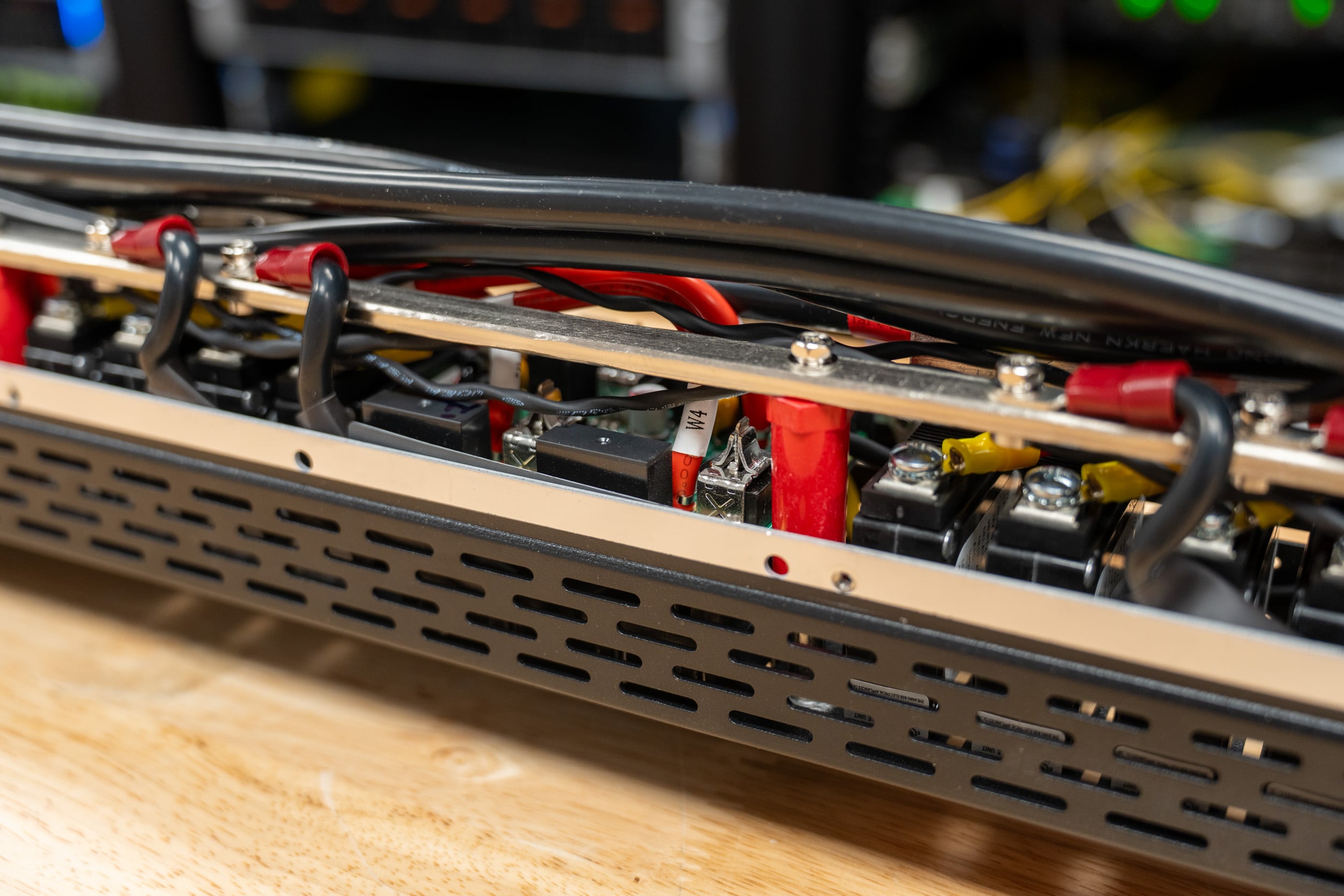
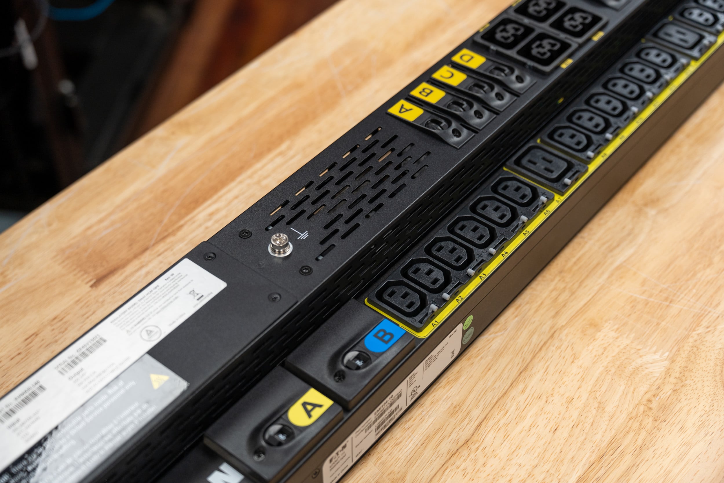
All models are three-phase Wye designs with what Eaton calls a near 1:1 outlet-to-breaker configuration: 21 branch breakers protecting 24 outlets. Outlets 1 through 12 each have a dedicated breaker (lettered A through M, skipping I and O). In the remaining twelve, three breakers each cover a pair of adjacent outlets: N for 13 and 14, R for 17 and 18, and U for 21 and 22, while the other six positions keep their own. So 18 of the 24 outlets are on a breaker of their own, and six share in pairs, which means a trip takes down one device, or at most two, rather than a six-outlet bank. Two input styles are offered: a corded model terminating in a 100A IEC-style 5100P6W connector (the EVMAXL100 in the manual) and a terminal-block model for permanently connected 140A service (EVMAXL140). Eaton specifies 100A or 140A branch-circuit protection upstream. With the cover off, the current this class is built to carry is obvious: heavy-gauge conductors and bus work feed each branch breaker, sized for a 100A or 140A three-phase input rather than the 30A-class internals most rack PDUs still use.

Inside the Eaton HDXL Rack PDU, heavy-gauge red and black conductors and bus bars feeding the branch breakers

Every outlet is Eaton’s C39, the combination receptacle the company introduced on the G3 Universal PDU, which merges the C13 and C19 outlet styles into one high-retention opening that accepts both C14 and C20 plugs. On the G3, Eaton split the loadout into 21 C14 and 21 C39; here, all 24 positions take either plug, which matters when a rack mixes 3200W server supplies with smaller items like switches. Branch breakers are rated to trip at 20A in US trim (16A EU), comfortably above the roughly 14A that a 3200W Titanium supply pulls at 230V. Inside, every outlet position sits behind a branch breaker, and because our units are the Managed version, each outlet also has its own relay for remote switching, so switching stays per outlet even on the three shared-breaker pairs.

Close-up of Eaton HDXL Rack PDU C39 outlets with lettered breaker labels and the Gigabit Network Module

Two management topologies span the four launch models. Metered Outlet (MO) units monitor at the input, branch, and individual outlet levels; Managed (MA) units add per-outlet switching on top of the same monitoring stack. Both carry Eaton’s Gigabit Network Module with an LCD, per-outlet status LEDs, and support for the optional Environmental Monitoring Probe, which reads temperatures from 0°C to 70°C with ±2°C accuracy, tracks humidity, monitors two dry-contact devices, and can be installed up to 50 meters away over Cat5. The units are rated IP20 and operate at ambient temperatures up to 60°C at altitudes below 1,000 meters, derating to 50°C at 3,000 meters.

Two Eaton HDXL Rack PDUs on the bench showing the Gigabit Network Module LCD, Ethernet ports, and C39 outlets

HDXL vs. G3 Universal PDU

Specification Eaton HDXL Rack PDU G4 Eaton G3 Universal PDU
Power
Capacity per PDU 56kW to 81kW 5kVA to 23kVA
Input 100A corded (5100P6W) or 140A terminal block Universal input, 12 cord options up to 60A
Phase configuration Three-phase Wye, 415/240V class Single-phase or three-phase by cord
Outlets and Protection
Outlets 24x C39 (accepts C14 and C20) 42 total: 21x C14, 21x C39
Branch protection 21 breakers, near 1:1 per outlet 6 color-coded outlet banks with breakers
Management
Topologies Metered Outlet (MO), Managed (MA) with per-outlet switching Single universal SKU; monitoring via EMP Gen2
Network and sensors Gigabit Network Module, LCD, optional EMP Daisy chaining, EMP Gen2
Availability
Launch 4 models, 2H 2026, standard from-stock offering Shipping (reviewed October 2023)


The spec sheet above makes it pretty clear that the G3 universal was geared toward mixed-rack environments where a variety of servers, storage, and switches may be involved. The HDXL, on the other hand, is a highly focused PDU that’s going after the high-power profile that GPU servers demand.

What We Can and Can’t Say Yet

Here’s the caveat we started with up top: our lab doesn’t have the high-voltage three-phase service these units require, so this isn’t our typical lab test. The HDXL Eaton sent has been racked, photographed, and inspected, but until we can put real load through them, we can’t speak to metering accuracy, breaker behavior, thermal performance under sustained draw, or the management experience under production conditions. We have, however, tested that with Eaton’s other PDUs and would expect that everything performs as advertised.

Eaton HDXL Rack PDU installed at the rear of a rack of Dell PowerEdge servers with power cords connected

One thing besides the design and build quality we can evaluate is the fit; these sit nicely in our older 42U Eaton racks without a problem, staying entirely out of the way.

Final Thoughts

The HDXL is power infrastructure catching up to what compute is already consuming. Enterprise AI systems now ship as 4- and 8-GPU servers that draw kilowatts instead of watts. When a single 4U server can carry more than 25kW of power supply capacity and eight power cords, the 23kVA PDU generation becomes the bottleneck. That’s the deployment this family was designed and built for. Eaton’s HDXL is dense, breaker-per-outlet (mostly), and standardized on an outlet that accepts both plug types a modern rack uses. If you’re speccing racks for dense enterprise AI, four or eight GPUs per box, the HDXL family belongs on the evaluation list, provided your facility can deliver the 100A-plus feeds it’s designed to distribute.

Eaton HDXL Rack PDU angled on the lab bench in front of the StorageReview server racks

Eaton Rack PDU G4 Product Page

The post Eaton HDXL Rack PDU Review: 81kW From a Single Zero-U PDU for AI Racks appeared first on StorageReview.com.

HP ZGX Fury Is Now Orderable: GB300 Superchip, 748GB Unified Memory, and a Red Hat AI Factory Plan for the Edge

HP ZGX Fury AI station tower in the StorageReview lab, showing the front mesh panel, ZGX badge, and front USB and audio ports HP ZGX Fury AI station tower in the StorageReview lab, showing the front mesh panel, ZGX badge, and front USB and audio ports

HP’s ZGX Fury AI station is now available to order, and HP paired the availability news with a collaboration with Red Hat and NVIDIA to put Red Hat AI Factory with NVIDIA on top of it. The ZGX Fury is HP’s take on NVIDIA’s DGX Station design, built around the GB300 Grace Blackwell Ultra Desktop Superchip with 748GB of unified memory and up to 20 petaFLOPS of FP4 compute, and HP is positioning it less as a personal workstation than as a shared inference box that a department, a factory floor, or a branch office can run without a data center behind it. We have one in the lab now, so a full review is coming; this is what HP has said so far.

HP ZGX Fury AI station tower in the StorageReview lab, showing the front mesh panel, ZGX badge, and front USB and audio ports

HP ZGX Fury Hardware: One GB300 Superchip, 748GB of Memory, Tower or 5U

The core of the system is the same silicon we tested in the MSI XpertStation WS300: one Blackwell Ultra GPU with 252GB of HBM3e at 7.1TB/s, tied to a 72-core Grace CPU with 496GB of LPDDR5X over NVLink-C2C. HP’s spec sheet fills in details the platform announcements skipped. The CPU memory is four 128GB SOCAMM modules delivering 396GB/s, and the Grace CPU is soldered to the host processor module rather than socketed. The two pools add up to the 748GB coherent space that lets the GPU address CPU memory directly, which is what makes trillion-parameter inference and fine-tuning of models in the 100 billion parameter class possible on a single box. HP’s footnote on those model sizes is that the harness quantizes at FP4.

Two embedded M.2 slots hang off the Grace CPU on PCIe 5.0 and hold the operating system in a software RAID 1 mirror. Two more M.2 slots come off the PCIe switch inside the ConnectX-8 SuperNIC and serve as a RAID 0 data volume, with 2TB or 4TB of self-encrypting NVMe chosen at purchase.

Networking is the ConnectX-8 with two QSFP112 ports at 400Gbps each, which can link two ZGX Fury systems together, plus a 10GbE RJ-45 for the host and a separate 1GbE RJ-45, Mini-DP, and micro-USB for the BMC. The rest of the I/O is workstation-normal: two USB-A and two USB-C ports up front, four more USB ports at the rear, audio jacks, a Kensington slot, and a C20 inlet for the power cord. There is no display output from the GB300 itself; HP offers an optional NVIDIA RTX PRO GPU to drive monitors so the Blackwell Ultra GPU stays dedicated to inference. The chassis is a tower that also ships with rails for a 5U rack slot, and HP uses liquid cooling with optimized airflow, which matches what we found on the MSI unit, where a 1,400W-rated loop kept the GPU at 71C under full load.

HP ZGX Fury Software: Ubuntu, Z Runtime, and Red Hat Certification

HP ships the ZGX Fury with Ubuntu 24.04 LTS and NVIDIA’s AI developer tools, an NVIDIA-approved partner BIOS and BMC firmware, and two HP-specific layers. HP Z Runtime is a pre-installed command-line tool for pulling, serving, and managing models locally, and HP Z Toolkit adds open-source frameworks, MLflow experiment tracking, and Ollama testing with discovery and sync across ZGX systems. The idea is that a team prototypes on a ZGX Nano and moves the same workflow to a ZGX Fury when it needs more memory, more throughput, or more concurrent users.

The new piece is Red Hat. HP says the ZGX Fury is certified for Red Hat Enterprise Linux and listed in the Red Hat Ecosystem Catalog today, and the two companies are developing what HP calls an open, enterprise-grade AI platform that runs Red Hat AI Factory with NVIDIA on the ZGX Fury. Red Hat AI Factory with NVIDIA is Red Hat’s packaging of RHEL, OpenShift, and Red Hat AI Enterprise with NVIDIA AI Enterprise for deploying models, agents, and applications across hybrid cloud. On the ZGX Fury, HP says the combination is meant to cut environment setup time and deployment risk, improve GPU utilization through optimized CUDA libraries, scheduling, and multi-GPU workload orchestration, and let developers offload compute to the box without changing their existing workflows. The platform is also being designed to run multiple AI workloads on one system with workload isolation and governance, which is how HP gets from a deskside machine to something IT can manage as edge infrastructure.

“The future of AI is moving closer to where people work, machines operate and critical decisions are made,” said Jim Nottingham, Senior Vice President and Division President of Advanced Compute and Solutions at HP. “Together with Red Hat and NVIDIA, HP is extending enterprise AI from the data center to the edge with an open, enterprise-grade inference platform designed to give customers greater choice, control and consistency as they deploy local AI factories.” Chris Marriott, Vice President of Enterprise Platforms and Solutions at NVIDIA, framed it the same way: running “powerful AI locally while maintaining the security, scalability, and consistency enterprises demand.”

The ZGX Fury is orderable now through HP; pricing was not disclosed in the announcement. The Red Hat AI Factory integration is a planned solution rather than a shipping SKU, and HP says customers will be able to evaluate it in a sandboxed environment on HP devices before moving to production, with timing, eligibility, and supported configurations still to come. The competitive picture is filling in quickly: MSI’s WS300 is shipping on the same superchip, and AMD’s Threadripper Halo Station is aimed at the same workloads. Our ZGX Fury review will put HP’s version of the platform through the same model and testing we ran on the MSI.

HP ZGX Fury AI Station

The post HP ZGX Fury Is Now Orderable: GB300 Superchip, 748GB Unified Memory, and a Red Hat AI Factory Plan for the Edge appeared first on StorageReview.com.
Samsung High NA EUV DRAM Set for 2028, With 12-Inch Photomasks and a Mistral AI Series D Lead

ASML TWINSCAN EXE:5000 High NA EUV lithography system with its panels open, the platform Samsung plans to use for DRAM production by 2028 ASML TWINSCAN EXE:5000 High NA EUV lithography system with its panels open, the platform Samsung plans to use for DRAM production by 2028

Samsung Electronics made two moves in two days that both point at the same problem: keeping its memory and foundry lines on the leading edge as AI demand outruns conventional scaling. On September 8, Samsung and ASML announced an expanded partnership under which Samsung will put ASML’s High NA extreme ultraviolet (EUV) lithography into high-volume DRAM manufacturing by 2028 and join the industry effort to move from 6-inch to 12-inch photomasks. A day later, at the South Korea and France state summit in Paris, Samsung announced a strategic partnership with Mistral AI to run the French developer’s models on-premises across its chip operations, along with a lead investment in Mistral’s Series D round.

Samsung High NA EUV for DRAM by 2028 and the 12-Inch Photomask Transition

Samsung says it plans to introduce ASML’s High NA EUV systems into future DRAM high-volume manufacturing by 2028, which the two companies describe as the first such deployment in the industry. High NA raises the numerical aperture of the projection optics from 0.33 to 0.55, and the tighter resolution is meant to extend the DRAM scaling roadmap by simplifying process steps that today require multiple patterning passes. Samsung laid out where that scaling is headed in its 3D memory roadmap at FMS 2026, and High NA is the lithography piece that has to be completed first.

ASML TWINSCAN EXE:5000 High NA EUV lithography system with its panels open, the platform Samsung plans to use for DRAM production by 2028

In parallel, Samsung is joining the industry initiative to develop a 12-inch photomask platform for High NA EUV. The 6-inch mask has been the standard for decades, but High NA systems use anamorphic optics that halve the exposure field, so printing a full-size die on a 6-inch reticle means stitching two exposures together. ASML and Samsung say the larger 12-inch format is expected to raise fab productivity, lower chipmaking costs, and remove those stitching constraints, letting manufacturers use High NA without the throughput penalty. Samsung says it will work with industry partners to develop the mask technologies and supporting infrastructure the new format requires, drawing on its experience running EUV in both memory and foundry production.

ASML TWINSCAN EXE:5000 High NA EUV lithography system with two technicians at the front panel

“The AI era is transforming the semiconductor industry and increasing the importance of technological innovation across the entire value chain,” said Young Hyun Jun, Vice Chairman and CEO of Samsung Electronics. “By further strengthening our collaboration with ASML, we are helping lay the foundation for the next generation of AI and semiconductor innovation.” ASML President and CEO Christophe Fouquet called Samsung “one of ASML’s most important innovation partners for many years,” and both companies said they expect to keep exploring collaboration in advanced memory and new manufacturing approaches.

Mistral AI Models Running On-Premises Inside Samsung’s Fabs

The second announcement puts Mistral’s models, including its flagship Mistral Large, to work inside Samsung’s semiconductor operations. Samsung says it will integrate Mistral’s AI services and solutions to develop customized on-premises models for what it calls intelligence-driven infrastructure, with the on-premises deployment chosen so that process technology and operational data stay entirely within Samsung’s own semiconductor infrastructure.

Mistral AI graphic with icons for regional control, third-party models, and data security on a blue grid

The stated targets are practical fab problems rather than chip design in the abstract. Samsung says it will apply targeted models to defect detection and equipment optimization, with the goal of accelerating development cycles, manufacturing precision, and yield stabilization across its advanced memory and logic chips. As process nodes get more complex, the company argues, fast data analysis inside the fab becomes essential, and Mistral’s stack is meant to change how its chips are designed and manufactured.

“Increasing complexities involved in AI chip design and manufacturing requires continuous innovation in semiconductor technologies,” Jun said, this time bylined as head of Samsung’s Device Solutions Division. Mistral co-founder and CEO Arthur Mensch said the company is “proud to support Samsung Electronics with our expertise in electronics and semiconductors, helping to improve how chips are designed and manufactured.”

Samsung also led Mistral’s Series D funding round, taking what it describes as a strategic equity stake to support long-term technology collaboration. Samsung did not disclose the round size or its share. The investment puts Samsung alongside its own lithography supplier on Mistral’s cap table: ASML led Mistral’s Series C exactly one year earlier, in September 2025, with a 1.3 billion euro investment for roughly an 11 percent stake. Mistral has been building out its own infrastructure as well, with Mistral Compute AI factories on NVIDIA GB300 NVL72 and a deepening collaboration with Dell on enterprise deployments.

Taken together, the two announcements show Samsung buying capability on both ends of the fab: the lithography that determines how small the next DRAM cell can get, and the models it wants watching the line once those tools are running.

Samsung Semiconductor

The post Samsung High NA EUV DRAM Set for 2028, With 12-Inch Photomasks and a Mistral AI Series D Lead appeared first on StorageReview.com.
QNAP TVS-hx77AX Brings NFS over RDMA and U.2 NVMe to Desktop ZFS NAS

Front view of the 16-bay QNAP TVS-h1677AX with twelve 3.5-inch SATA bays and four U.2 NVMe slots Front view of the 16-bay QNAP TVS-h1677AX with twelve 3.5-inch SATA bays and four U.2 NVMe slots

QNAP has introduced the TVS-hx77AX series, a new line of desktop ZFS NAS systems combining AMD Ryzen 7000 series processors with DDR5 memory, U.2 NVMe storage, and NFS over RDMA support. The family includes the 16-bay TVS-h1677AX, 12-bay TVS-h1277AX, and 8-bay TVS-h877AX, and QNAP is aiming all three at video collaboration, virtualization, and small-scale AI work rather than the home NAS market.

QNAP TVS-hx77AX series flagship TVS-h1677AX on a desk with its four U.2 NVMe PCIe 4.0 x2 slots highlighted above the SATA bays

All three systems run QuTS hero and ship with 16GB of DDR5 memory, expandable to 192GB across four UDIMM slots with optional ECC support. QNAP’s spec sheet lists the processor as a six-core, 12-thread Ryzen 5 7000 series part with a 5.1GHz boost clock, and the product page identifies it as the Ryzen 5 PRO 7645. Networking includes two 10GBASE-T and two 2.5GbE ports, while three PCIe Gen 4 slots can accommodate additional network adapters or discrete GPUs. QNAP supports 25GbE expansion through an optional adapter, which is also the path to NFS over RDMA with a compatible SmartNIC.

The storage configuration changes with each model: The TVS-h1677AX combines twelve 3.5-inch SATA bays with four U.2 NVMe slots, the TVS-h1277AX has eight SATA bays and four U.2 slots, and the smaller TVS-h877AX uses six SATA bays and two U.2 slots.

QNAP TVS-h1677AX, TVS-h1277AX, TVS-h877AX Specifications

Specification TVS-h1677AX TVS-h1277AX TVS-h877AX
CPU AMD Ryzen 5 7000 series, 6-core/12-thread, up to 5.1GHz AMD Ryzen 5 7000 series, 6-core/12-thread, up to 5.1GHz AMD Ryzen 5 7000 series, 6-core/12-thread, up to 5.1GHz
Graphics AMD Radeon Graphics AMD Radeon Graphics AMD Radeon Graphics
Memory 16GB DDR5, up to 192GB, 4x UDIMM, optional ECC 16GB DDR5, up to 192GB, 4x UDIMM, optional ECC 16GB DDR5, up to 192GB, 4x UDIMM, optional ECC
SATA Bays 12x 3.5-inch SATA 8x 3.5-inch SATA 6x 3.5-inch SATA
U.2 NVMe 4x U.2 PCIe Gen 4 x2 4x U.2 PCIe Gen 4 x2 2x U.2 PCIe Gen 4 x4
Networking 2x 10GBASE-T, 2x 2.5GbE 2x 10GBASE-T, 2x 2.5GbE 2x 10GBASE-T, 2x 2.5GbE
25GbE Optional adapter Optional adapter Optional adapter
PCIe Expansion 3x PCIe Gen 4 (x8/x4, x4, x4) 3x PCIe Gen 4 (x8/x4, x4, x4) 3x PCIe Gen 4 (x8/x4, x4, x4)
USB 2x USB-C 10Gbps, 2x USB 2.0 2x USB-C 10Gbps, 2x USB 2.0 2x USB-C 10Gbps, 2x USB 2.0
HDMI HDMI 1.4b, up to 4096 x 2160 at 30Hz HDMI 1.4b, up to 4096 x 2160 at 30Hz HDMI 1.4b, up to 4096 x 2160 at 30Hz
Power Supply 500W, 8-pin (6+2) PCIe cable 500W, 8-pin (6+2) PCIe cable 500W, 8-pin (6+2) PCIe cable
Typical Power (QNAP, drives populated) 164.03W 106.38W 105.12W
Dimensions (H x W x D) 294.3 x 369.9 x 319.8mm 225.2 x 369.9 x 319.8mm 225 x 292.9 x 319.8mm
Warranty 5 years 5 years 5 years

QNAP TVS-h1677AX

The TVS-h1677AX is the largest system in the series, with twelve 3.5-inch SATA bays and four 2.5-inch U.2 NVMe slots for a total of 16 drive bays. Each U.2 slot uses a PCIe Gen 4 x2 interface and supports compatible PCIe Gen 4 and Gen 5 U.2 SSDs. SATA bays also support 2.5-inch SATA SSDs. One operational note from QNAP’s spec sheet: a U.2 SSD can only be hot-swapped if it was installed before the system booted, so a drive added while the NAS is running needs a shutdown to be replaced later.

Front view of the 16-bay QNAP TVS-h1677AX with twelve 3.5-inch SATA bays and four U.2 NVMe slots

Expansion comes through three PCIe Gen 4 slots. The primary slot can operate at x8 when the adjacent slot is unused, or x4 when both are populated, while the remaining slots operate at x4. QNAP also includes a 500W power supply with an 8-pin 6+2 PCIe power cable for a discrete GPU. The TVS-h1677AX measures 294.3 x 369.9 x 319.8mm, weighs 10.98kg, and is cooled by three 80mm system fans plus two 60mm CPU fans.

QNAP TVS-h1277AX

The TVS-h1277AX reduces the SATA count to eight bays while retaining the same four U.2 PCIe Gen 4 x2 slots as the larger model. It therefore provides 12 total drive bays while keeping the same 192GB maximum DDR5 memory capacity, dual 10GBASE-T ports, dual 2.5GbE ports, and three PCIe Gen 4 expansion slots.

Front view of the 12-bay QNAP TVS-h1277AX with eight SATA bays and four U.2 NVMe slots

Its shorter chassis measures 225.2 x 369.9 x 319.8mm. QNAP lists typical operating power consumption at 106.38W with the drives fully populated, compared with 164.03W for the larger TVS-h1677AX under the same stated test condition. Both use 500W power supplies.

QNAP TVS-h877AX

The TVS-h877AX is the smallest member of the family, combining six 3.5-inch SATA bays with two U.2 NVMe bays. Its U.2 interfaces run at PCIe Gen 4 x4, compared with the four Gen 4 x2 U.2 slots used by the TVS-h1277AX and TVS-h1677AX, so each of its two NVMe drives gets twice the lanes.

QNAP TVS-h877AX with its six SATA drive trays and two U.2 NVMe trays pulled partly out of the chassis

The smaller chassis measures 225 x 292.9 x 319.8mm and weighs 8.88kg, with two 80mm system fans instead of three. QNAP’s typical operating figure for it is 105.12W with drives populated. It retains the same dual 10GBASE-T and dual 2.5GbE networking configuration, three PCIe Gen 4 expansion slots, 192GB maximum memory capacity, and 500W power supply as the larger systems.

NFS over RDMA and 25GbE Expansion

NFS over RDMA is a major addition to the TVS-hx77AX series; instead of moving NFS traffic through the conventional CPU networking path, RDMA permits direct memory access between systems, reducing CPU involvement in data transfers. QNAP is targeting the feature at AI training, virtualization, and high-resolution video workflows, and says its reference configuration sustained more than five simultaneous ProRes 4444 4K streams. The feature needs QTS 5.2.6 or QuTS hero h5.2.6 or later, and QNAP recommends pairing it with a RoCE-capable card.

The TVS-hx77AX series includes dual 10GBASE-T and dual 2.5GbE ports, while 25GbE connectivity can be added through a compatible PCIe adapter. QNAP’s NFS over RDMA configuration uses its QXG-25G2SF-BCM 25GbE SmartNIC. The three PCIe Gen 4 expansion slots can also accommodate additional network adapters or discrete graphics cards, giving the systems room for higher-speed networking or GPU acceleration. GPU passthrough is supported as well, allowing compatible graphics hardware to be assigned directly to virtual machines.

QNAP has published lab figures for the TVS-h1677AX with the network slots filled: 12,174MB/s sequential read and 11,065MB/s sequential write over SMB, and 1,140,212 random read IOPS and 782,483 random write IOPS over iSCSI, each across six 25GbE ports. Those are QNAP’s numbers, not ours, and the test system was upgraded to 64GB of memory with three QXG-25G2SF-CX6 adapters, four Samsung PM9A3 U.2 SSDs, and twelve SATA SSDs in RAID 5, so it does not represent the 16GB, HDD-populated configuration most buyers will start with.

Hybrid Storage and QuTS hero

The TVS-hx77AX series runs QNAP’s ZFS-based QuTS hero operating system, now at QuTS hero h6.0. Its hybrid drive layout combines high-capacity SATA storage with dedicated U.2 NVMe slots, and the pairing is meant for Qtier for QuTS hero, the tiering feature that moves active data to the NVMe tier and cold data to hard drives. Qtier requires h6.0, and QNAP’s product page still lists it as upcoming for this series, so buyers should treat automatic tiering as a pending feature rather than a day-one one.

QuTS hero h6.0 also brings immutable snapshots, ZFS self-healing, and High Availability Manager, which clusters two identical NAS units with one active and one passive for failover and a recovery time objective QNAP puts under 60 seconds. We tested that failover on a pair of TS-h765eU units last month and covered the process on video, and a matched pair of TVS-hx77AX systems would work the same way.

QNAP High Availability Manager in QuTS hero h6.0 showing a healthy two-node cluster with active and passive nodes

Qsirch adds AI-assisted enterprise search with Retrieval-Augmented Generation support, which can connect with cloud or on-premises large language models and use natural-language queries to search content stored on the NAS.

QNAP TVS-hx77AX Availability

The TVS-hx77AX gives QNAP three desktop ZFS configurations sharing the same Ryzen 7000, DDR5, networking, and PCIe foundation while varying the SATA and U.2 storage layout. The TVS-h1677AX provides the highest drive count, the TVS-h1277AX retains four U.2 slots in a smaller chassis, and the TVS-h877AX reduces the overall bay count while using PCIe Gen 4 x4 for its two U.2 slots.

All three models are available now with a five-year standard warranty, sold as the TVS-h1677AX-R5-16G, TVS-h1277AX-R5-16G, and TVS-h877AX-R5-16G.

QNAP TVS-h1677AX Product Page

QNAP TVS-h1277AX Product Page

QNAP TVS-h877AX Product Page

The post QNAP TVS-hx77AX Brings NFS over RDMA and U.2 NVMe to Desktop ZFS NAS appeared first on StorageReview.com.

HPE Alletra Storage MP B10000 10.6.0 Arrives With Six-Node Scale-Out and Agentic Support Automation

HPE has made the 10.6.0 software release for the Alletra Storage MP B10000 generally available, landing inside the Q3 2026 window the company set when it previewed the release in May. HPE is also calling it Release 6 in its channel materials. The update takes the B10000’s disaggregated block-and-file architecture from four controller nodes to six, adds an agent-based support automation layer, folds real-time ransomware detection for both protocols into the array itself, and raises the platform’s capacity guarantee. HPE’s pitch is that unified storage has usually meant separate block and file products sharing a management pane, and that the B10000 consolidates the two on one shared-everything design where compute and capacity scale independently.

Front of two HPE Alletra Storage MP B10000 nodes with HPE bezels installed in a rack

Six-Node Scale-Out and Workload Scope

The B10000 decouples controller compute from the capacity shelves behind it, so an organization can add performance or capacity separately as I/O profiles and footprints diverge, rather than buying both at once, as a dual-controller array requires. With 10.6.0, a cluster can grow from a single node to six in single-node increments. HPE puts the gain at a 50 percent performance increase over the previous four-node maximum, and says a six-node cluster can survive two simultaneous node failures without a service interruption. Customers that started on a switchless two-node configuration can also convert to a switched cluster without disruption, so a small deployment can grow into a larger cluster without a rebuild. Against a traditional scale-up array, HPE cites 40 percent TCO savings and a 45 percent reduction in energy consumption for the scale-out design, figures that come from HPE’s own substantiation rather than third-party testing.

The release also updates the HPE StoreMore Guarantee that backs the platform’s data reduction. HPE says the guaranteed effective capacity ratio moves to 5:1, up from 4:1, so a buyer sizing a B10000 can plan on more usable capacity per raw terabyte than before. As with any vendor guarantee, the ratio is workload-dependent, and the terms sit in HPE’s program documentation rather than the release itself.

HPE is positioning the platform for standard enterprise block workloads alongside adjacent unstructured file services, and 10.6.0 expands the file side with greater file capacity and snapshot support. HPE names SAP HANA and containerized applications as the workloads that need both protocols on the same system. It is not intended to replace the Alletra Storage MP X10000, which remains the company’s object platform for high-bandwidth AI, machine learning, EDA, and large-scale media pipelines. The aim of 10.6.0 is to consolidate general enterprise block and file data into a single system so that the two no longer reside in separate operational silos.

Agentic Support Automation

The more novel piece is what HPE calls agent-based support automation. Instead of threshold alerts that fire only after a metric crosses a fixed limit, the release deploys a set of specialized agents for detection, analysis, recommendation, and remediation that run continuously against the array’s telemetry. HPE says the system processes billions of log entries and sensor metrics a day, using GPU-accelerated inference to spot behavioral drift and correlate it with the workload responsible. The example HPE gives is uneven capacity exhaustion, where aggregate utilization looks healthy while one process quietly consumes the remaining headroom; the agents are meant to catch the pattern early and provide the administrator with a recommended fix, or, in some cases, carry out the remediation before an outage. HPE’s channel notice puts a qualifier on that last step: the remediation agent implements fixes with approval, so the autonomous path still runs through an administrator. Fleet telemetry and control stay in HPE’s Data Services Cloud Console, the GreenLake management plane for the Alletra line.

Cyber Resilience Built Into the Array

Data protection in 10.6.0 is part of the platform, not a downstream target. The B10000 now runs real-time ransomware detection natively on both the block and file access paths, and HPE says its Cybersecurity Center of Excellence validated the detection against more than 100 of the most common ransomware strains. The release adds continuous security posture monitoring, which checks the array’s security configuration in the background and flags drift for audits, and it protects immutable snapshot schedules from being altered. Immutable snapshots, integration with SIEM and XDR tooling, and role-based access controls with MFA, FIPS 140-3 compliance, and DISA-approved STIG hardening guidance round out the on-array controls, mapped to the NIST Cybersecurity Framework we walked through in our B10000 cyber resilience deep dive.

Zerto dashboard protecting VMs on HPE Alletra Storage MP B10000 in the StorageReview lab, showing six VPGs at a one-second RPO

That array-level detection feeds a layered design. HPE Zerto Software supplies VM-level inline detection and continuous data protection for application recovery, and the release adds backup APIs plus integrated application-consistent backup to HPE StoreOnce for immutable retention, without an ISV in the path. Spreading detection, replication, and isolated retention across separate tiers is how HPE argues the platform avoids a single point of recovery failure during an attack.

The timing aligns with a run of third-party recognition that HPE is leaning on for the B10000. HPE cites IDC data calling it the fastest-growing all-flash block storage array, and HPE landed in the Leaders quadrant of the 2026 Gartner Magic Quadrant for Enterprise Storage. What 10.6.0 adds to that story is the ability to scale a unified block-and-file system out to six nodes, monitor it with an agent framework rather than a page of thresholds, and keep ransomware detection on the array instead of bolting it on afterward. For enterprise IT shops trying to collapse a general-purpose block array and a file server onto one platform, that is a more concrete consolidation path than the shared-console version of unified storage.

HPE Alletra Storage MP B10000

The post HPE Alletra Storage MP B10000 10.6.0 Arrives With Six-Node Scale-Out and Agentic Support Automation appeared first on StorageReview.com.
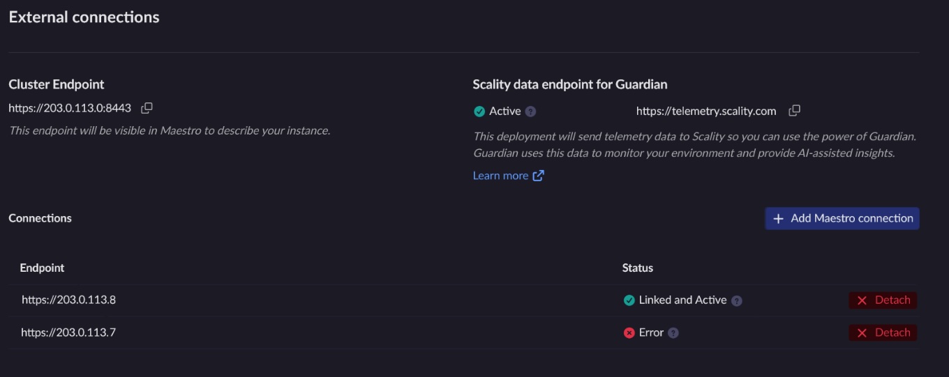
Qualcomm and Amazon Sign Multi-Generation Deal for Custom AI Inference Silicon and 1.6T Optical Interconnects

Qualcomm Technologies and Amazon have entered into a multi-generation collaboration to deliver customized silicon at scale for AWS’s AI data centers, with AI inference as the primary target. The agreement pairs Qualcomm’s power-efficient processing, silicon design, and system-level integration with Amazon’s AI infrastructure, and is aimed at the compute, memory bandwidth, networking, and energy constraints that come with running inference at hyperscale volume. Neither company named specific parts, delivery dates, or financial terms.

Qualcomm Dragonfly AI300 data center render with rows of racks and the Dragonfly AI300 badge

Custom Silicon and 1.6T Optical Connectivity

Beyond the compute silicon, the two companies are co-developing high-performance optical connectivity for Amazon’s data center networks, with solutions reaching 1.6T and future generations on the roadmap. That work draws on Qualcomm’s high-speed SerDes and optical DSP technologies, the same connectivity portfolio the company laid out at its June Investor Day alongside the Dragonfly C1000 CPU and AI300 accelerator. The intent is to keep network bandwidth from becoming the bottleneck as inference clusters scale out across racks.

The relationship also runs in the other direction. Qualcomm plans to deepen its use of AWS AI infrastructure, including Amazon Bedrock, for its electronic design automation (EDA) workloads, with the stated goal of shortening chip design cycles. That puts AWS compute behind the modeling and verification work for the very silicon Qualcomm will be building for Amazon.

What the Deal Signals

Executives on both sides framed the agreement around compute and connectivity advancing together. “As AI demand accelerates, data center infrastructure will require advances in both computing and connectivity to deliver greater performance with more efficiency,” said Cristiano Amon, President and CEO of Qualcomm Incorporated. Prasad Kalyanaraman, Vice President at AWS, said the collaboration “builds on a strong foundation of partnership” and that “by working together on customized silicon and advanced connectivity, we’re delivering more performant, efficient, and cost-effective infrastructure for our customers.”

The announcement lands as Qualcomm pushes hard into the data center. The June Investor Day put a CPU, a roadmap of AI200, AI250, and AI300 inference accelerators, and a connectivity portfolio on the table, and the company closed its acquisition of Modular in July to give that silicon a software stack that does not depend on CUDA. AWS already designs its own Trainium and Inferentia accelerators through Annapurna Labs, so the open question is where Qualcomm-built silicon fits alongside those parts. The release does not say, but a multi-generation commitment from the largest cloud provider is the strongest customer signal Qualcomm’s data center business has shown so far.

The post Qualcomm and Amazon Sign Multi-Generation Deal for Custom AI Inference Silicon and 1.6T Optical Interconnects appeared first on StorageReview.com.
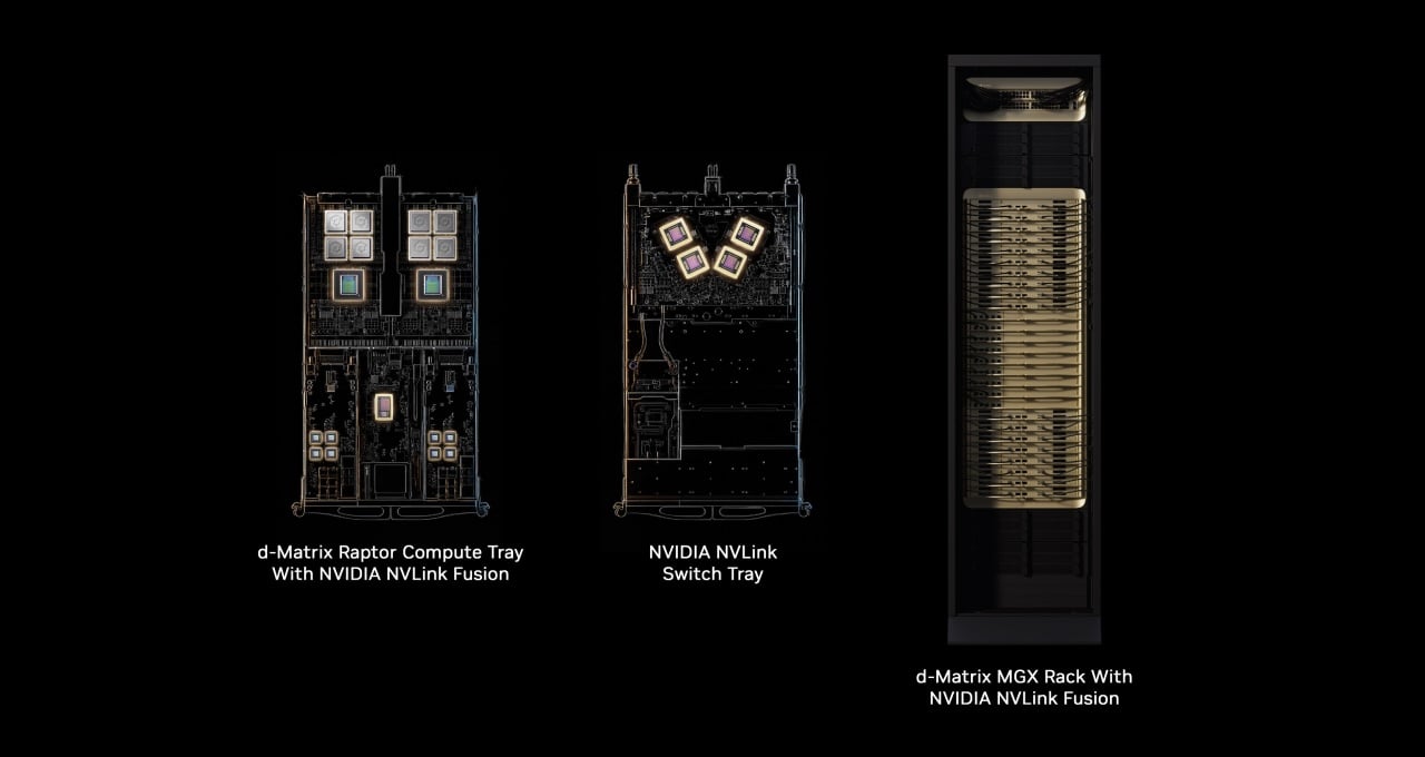
❌